This thread has been locked.

If you have a related question, please click the "Ask a related question" button in the top right corner. The newly created question will be automatically linked to this question.

UCC23313: Switching frequency range of the optocouplers

Part Number: UCC23313
Other Parts Discussed in Thread: UCC28950, UCC5350, UCC21520, UCC21225A, TIDA-00446

Hi team , 

I'm looking at UCC23313 gate driver part and another manufacturers parts for drive the mosfet.

How can I understand what the frequency range of the optocoupler is?

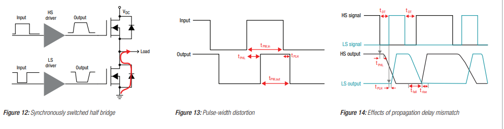
For example what does 

  •  propagation delay
  •  part-to-part delay matching
  •  pulse width distortion 

    terms mean?

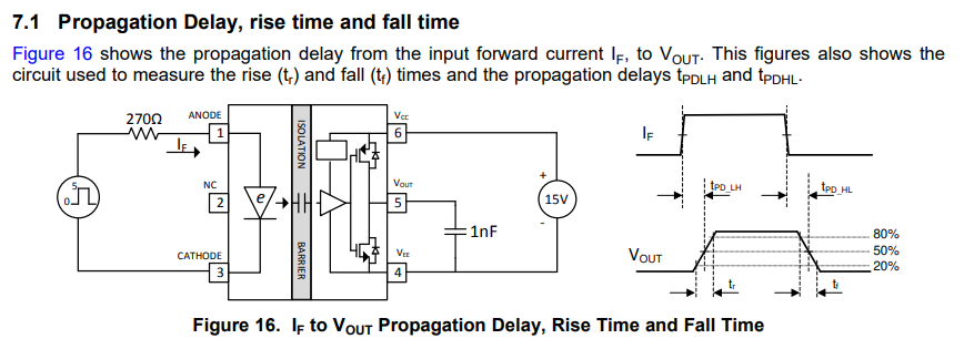
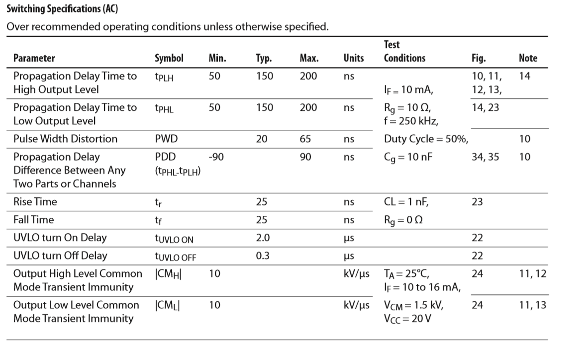
    And there is a figure below of the HCPL3180 gate drivers IC ,
    So can this IC & the UCC23313 work in 150kHz %90 duty cylce?


Best Regards 


  • Hi Fukan,

    That is a great question.

    Furkan Eroglu said:
    So can this IC & the UCC23313 work in 150kHz %90 duty cylce?

    Short answer: Yes, UCC23313 can operate at 150kHz.

    Long answer: Yes, depending on the load/device you are driving. the D-1 off cycle would represent ~660ns pulse width, and UCC23313 is certainly capable of this.

    Furkan Eroglu said:
    How can I understand what the frequency range of the optocoupler is?

    UCC23313 can operate >150kHz no problem. There is a reason the datasheets don't just provide frequency range like that. Its very dependent on design.

    I will give more information below:

    Furkan Eroglu said:

    what does 

    •  propagation delay
    •  part-to-part delay matching
    •  pulse width distortion 

    terms mean?

    Propagation delay is the delay from your input to the output of the gate driver, 50% of the high-value of input to 50% of the high value of output (or low value).

    Part-to-part delay matching is a measure of, if you have a bin of the same gate driver IC, how closely will all of their prop. delays match?

    Pulse-width distortion is the measure of the difference between rising and falling delays. 

    Dead time is the time when both high-side/low-side are OFF (e.g. half-bridge, full bridge). As dead time increases, efficiency decreases.

    The purpose for this is to provide margin. You want to give enough safe dead time margin so that you ensure that there high and low-side fets are conducting, which is a short circuit and can lead to catastrophic damage to the FETs and rest of system.

    Essentially, you want these numbers to be as low as possible. But why? The short story is you can increase system efficiency by minimizing deadtime, if you are driving half bridge, full bridge etc and have same driver for driving high and low side. 

    If your rise and fall times aren't matched exactly, leading to higher pulse-width distortion, you have to increase deadtime, as if the fall time is longer, you have to give extra margin to ensure both aren't on at same time.

    If your typical prop delay is very low, but your part-to-part delay matching is very poor, thats just as bad. You still have to provide increased deadtime in that case.


    Furkan Eroglu said:
    How can I understand what the frequency range of the optocoupler is?

    The max operating frequency of a SINGLE gate driver is basically dependent on how fast you can drive the load. The critical parameters would be rise/fall times of output. This is dependent on load, peak source/sink currents,VDD, and this is specced with a fixed load and VDD. The test bench that is used to characterize these parameters is here in section 7.1 of datasheet. You'll notice the HCPL3180 also specified CL of 1nF.

    If you are making half-bride/ full bridge implementation with multiple gate drivers, the the pulse-width distortion becomes important parameter that limits  the frequency of operation. Because the minimum amount of deadtime you must have in your circuit will limit the frequency of the system. 

    Additionally, POWER dissipation of the gate driver can also limit the max operating frequency. This scales with frequency and the size of the load (larger gate charge).

    Power ratings for UCC23313 are in section 6.4 of the datasheet

    Power equations are in the datasheet section 10.2.2.3 or 9.2.2.3 depending on PDF or HTML version.

    With that being said, UCC23313 has superior timing parameters to the Avago/Broadcom part, so UCC23313 is capable of operating with higher frequency than the other part.

    Just to take a quick look, the part-to-part prop-delay matching and pulse-width distortion are signifiantly lower. Apart from that, due to the type of isolation used, UCC23313's timing will stay constant. The Broadcom part's timing performance will worsen over time due to the aging of the opto-coupler. 

    To be frank, UCC23313 is a better choice to design for lower dead-time, higher frequency operations.

    In summary, UCC23313 can operate >200kHz and can support higher frequency and lower dead-time for the same load and VDD than the HCPL3180. Keep in mind the important parameters: Load, rise/fall times, pulse width distortion, part to part prop delay skew when determining the maximum frequency

    The figures for timing are from this excellent resource linked below. It specifically targets SiC/IGBT applications, but is just as helpful for learning about driving MOSFETs. recommend to take a look. Its a great resource to keep on-hand to explain the tradeoffs and critical parameters. http://www.ti.com/lit/ml/slyy169/slyy169.pdf#page=13

    I hope this helps. If this has answered your question, please let me know by clicking the green button. And let us know if you have any more questions!

    Best

    Dimitri 

  • Thank you  , nice answer you explained very well sir.

    If it won't be a problem for you, I would like to further elaborate my content.
    I will use this Opto-couplers in the UCC28950 PS-FB circuit.

    Can I even ask in the following way, what if I want to run the mosfets on
    %90 duty cycle ,
    100kHz Switching Frequency and with 210nC Gate capacity of the mosfet additional
    if I want to perform this operation with bootstrap, can it cause problems
    by using the UCC23313 , can you help me with this?

    yours affectionately.

    Furkan

  • Furkan,

    First: If you are using UCC28950, you do not necessarily have to use an opto-compatible gate driver like UCC23313. The opto-emulated/opto-coupler based designs require a higher forward current (7-16mA for this gate driver) which may require extra buffers. And as far as interlock function with multiple opto-emulated gate driver, it is not required from the perspective of the controller.

    You can also select a single or dual channel CMOS-input isolated gate driver that we offer, which could simplify your design. Since the controller you use already has programmable dead-time, this feature is not required in your gate driver. If you pick one with programmable dead-time, you can disable it as well.

    Example: UCC5350 (single channel) 

    Dual Channel: UCC21225A (basic isolation) or UCC21520 (reinforced)

    You can use a bootstrap circuit even with the max 90% duty cycle of high-side, but you will want to pay extra care to selection of the components. With so little time to charge the large bootstrap capacitor required, the peak current will increase compared to 50% fixed duty, and reverse recovery characteristic of the bootstrap diode becomes pronounced and can cause problems.

    The referenced App note for UCC28950 expresses concern for using bootstrap diode in this case and gives some details on what happens.

    We have an excellent resource on bootstrap circuit design here that gives the design methodology, which I recommend to take a look at.

    When selecting the bootstrap diode, select a fast-recovery Silicon diode or Schottky. You will want as low reverse recovery charge as possible when the duty cycle is that high.

    Another option is to use transformer-based isolated supply such as fly-back or push-pull converter which doesn't have limitations of bootstrap in applications of high-duty cycle, but this adds extra components and BOM cost compared to a bootstrap circuit. Transformer-based converter can also be used to generate the isolated bias which is used for low-side drivers. Since they don't rely on switching to recharge a bootstrap cap, they are capable to support all the way up to 100% duty cycle.

    We have some reference designs utilizing SN650x push-pull converter to generate btoh isolated high-side and low-side bias, in this reference design, its SN6506B

    Reference Design Page for TIDA-00446: http://www.ti.com/tool/TIDA-00446

    Schematic: http://www.ti.com/lit/df/tidrij3/tidrij3.pdf

    App note: http://www.ti.com/lit/ug/tiduaz0c/tiduaz0c.pdf#page=3

    I hope this helps. If this has answered your question, please click the green button. If you have more questions, let me know!

    Best regards,

    Dimitri

  • Thank you ,
    I will order one of these IC today and tomorrow 
    but there is still something I do not understand about the UCC23313 , 

    You say that ; The opto-emulated/opto-coupler based designs require a higher forward current (7-16mA for this gate driver) which may require extra buffers.

    But 

    The output current of the UCC28950 isn't enough already for the forward current of the UCC23313? Cause UCC28950's output currents it's almost 200mA 


    I could not fully understand this, but already UCC21220 etc. I wanted to focus on drivers, which was a reason.

    Thank you for you suggestions again.


    Furkan

  • Hi 

    Furkan Eroglu said:

    The output current of the UCC28950 isn't enough already for the forward current of the UCC23313? Cause UCC28950's output currents it's almost 200mA 

    You are correct: UCC28950 has the drive strength to drive the opto-emulated (TI) and opto-coupler based gate driver. In the general case from a typical MCU, it might not be supported.. You can use UCC23313 and select the proper ext resistors but theres not really a reason to choose that over a CMOS input gate driver.

    If this answered your question, please click the green button. Otherwise please let me know your additional questions.

    Best

    Dimitri

  • Thank you for helping sir!
    Was a very nice explanation thank you for all.


    Have a good day!

    Regards 

    Furkan

  • You are welcome Furkan,

    A colleague pointed some things out that I should clarify on your questions.

    1) UCC28950 has VDD 8-12V, so a gate driver that can support up to this input voltage level is required. Because of this, my earlier recommendation UCC21220 for dual channel option will not work, its input voltage range is up to 5V. This was an oversight on my part.

    I will revise the earlier comment to reflect this. For dual channel option, please take a look at, UCC21225A (basic isolation) or UCC21520 (reinforced). With the compatible input voltage range, UCC28950 and the gate driver input side can run off the same supply.

    2) A CMOS-input gate driver would be best because the UCC28950 requires higher than usual external current limiting resistors because of the high VDD up to 12V. We recommend to use non opto-compatible gate driver in your application.

    3) Earlier, you mentioned your FET's total gate charge was 210nC. We noticed this seems quite high than typical (usually order of 10s of nC). Could you let us know the FET part number you plan on using? And also to double check that value?

    Because the power dissipation scales with gate charge, VDD, Frequency, the power dissipation in the driver will be quite high driving a 210nC cap at typical 15V, my colleague noted >300mW power dissipation in this setup. I increase the emphasis on thermals. Please make sure to calculate the thermals to ensure the junction temperature will not exceed recommendation during operation. Note that different packages will have different

    ψjb

    parameter. For example, in case of IC UCC53x0 parts, both D and DWV package could be available for same part. 

    Can you double check on the gate charge and let me know? 

    Best

    Dimitri james

  • thank you for warning me about this, to be honest I'm a almost 3-month candidate in the power electronics industry. and there is no one to help me in the workplace where I worked. I act with your ( TI team's ) suggestions. so I try to understand all the words you say carefully and especially by repeating them.

    If we go back to our topic.

    IRFP460's mosfet wich has Max=170nC gate charge.

    I made the selection of the driver as follows, please correct it if I have a mistake.

    • 1-) The estimaded current required to properly drive my Mosfet is

     170nC/((31ns+62ns)/2) = 3.65A 

    Drivers with all gate current above this provide the first condition to drive this mosfet.

    • 2-) Does the driver need isolation?

    yes, because the grounds of the primary and the drivers are seperated.

    • 3-) Can the driver's operating frequency carry the frequency of the signals almost 100kHz? 

    for example ; yes , because in the datasheet of the UCC23313 or another part can we understand that he can operate at >200kHz.
    (provided that the gate capacity is also taken into account).

    I usually choose the driver for mosfet by doing the steps I mentioned above. I mean, I am doing it right or wrong, I do not know it yet. So if I did not ask you, I would buy the UCC23313 driver.

    so now I am totally waiting for your suggestions.

    thank you so much for everything


    Furkan 


  • Furkan,

    You can use use both CMOS-input or opto-emulated. We recommend to use CMOS-input. Opto-emulated devices are essentially for drop-in replacements for legacy designs that used optocouplers. For new designs, typical CMOS-input is easier to integrate.

    The parts we recommend to look at are UCC21225A (basic isolation) or UCC21520 (reinforced). UCC5350 would also work, but its a single channel driver.

    Regarding your steps 1-3: The selection for Isolation (basic vs. reinforced) ratings come from the specs of your systems e.g. bus voltage. The need to meet certain functional safety standards can dictate this too.

    Here is a good resouce on the isolation ratings: http://www.ti.com/lit/wp/slyy063/slyy063.pdf

    Another step: What is the topology/design, type of device you are driving, etc. Better design with single or dual channel gate driver?

    If driving IGBT for example, some drivers target IGBTs specifically with special protection features. Do i need any signalling back to the controller?

    Another step can be to consider special features of the gate driver from the high-level/system-level perspective. For some cases, gate drivers integrate protection features that otherwise would be external on the PCB which can be very convenient.

    Yes, Vishay IRFP460 has quite high total gate charge and seems to be an older device.

    Are you able to choose a different Mosfet/superjunction mosfet with lower gate charge?

    Best

    Dimitri

  • I have this mosfet right now, after I drive this, I will try to drive the mosfet with a lower gate capacity.
    But if you have suggestions, I would be happy both in terms of cost and performance.

    thank you so much for everything.

    Regards

    Furkan E.

  • Furkan, 

    I can't make a part suggestion as i dont know your full system, but I'll share some suggestions on how to find and choose MOSFET.

    First, Digikey (or mouser, or arrow). This link to Single channel MOSFETS.

    Expand the filters, then you can filter by QG, VDS, ID, RDSON. And it can show the multiple manufacturers and price you out directly.

    You can also use the site of MOSFET manufacturer to look at their product lines. 

    Other idea is for the device you are using, you can look at the reference design for the gate driver or possibly the controller.

    Use design and development tab to look at the reference designs using that gate driver, and search in the BOM for the FET/IGBT used in the design. In the case of UCC21520

    In UCC21520 reference design case they used IPP65R190C7, 650V mosfet w/ 23nC gate charge. You can use that as a basis or select that same part if it works for you.

    I hope this helps, if you have more question please let us know.

    Best

    Dimitri