This thread has been locked.

If you have a related question, please click the "Ask a related question" button in the top right corner. The newly created question will be automatically linked to this question.

MOSFET drive current question

Genius 3870 points

Hi ,

I read your answer on this thread https://e2e.ti.com/support/power-management/f/196/t/892573?tisearch=e2e-quicksearch when I search for method of calculating mosfet gate drive current. 

the two PDF you recommend are very useful, and I have some questions about them.  

Q1: In SLUA882, there are Assumptions that " Vgs(miller) ≈ Vgs(th) = 0.5*V_drvIg2,3 = 0.5* Ig_peak" in order to simplify the equations to get peak current of gate driver.  But I am not very sure  whether those assumptions are reasonable or conditionnally reasonable. 

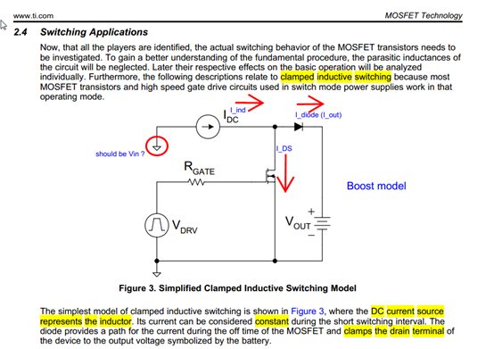
Q2: In slua618a, section 2.4, fig 3, I guess this simplified clamped inductive switching model comes from general BOOST converter topology?   If so, I think the left terminal of current soucre  IDC (the inductor) should be connected to Vin rather than GND. As I marked red circle below. How do you think ?

Thank you .

  • Hi Yi, I work with Don.

    Those are good questions!

    yi xiao said:

    Q1: In SLUA882, there are Assumptions that " Vgs(miller) ≈ Vgs(th) = 0.5*V_drvIg2,3 = 0.5* Ig_peak" in order to simplify the equations to get peak current of gate driver.  But I am not very sure  whether those assumptions are reasonable or conditionnally reasonable. 

    The Report you reference in Q2 goes into more details about the assumptions on pg8, namely temp, parasitics, gb. and shows how Vgs_miller is calculated like this.

    Please see Appendix A for more details

    yi xiao said:
    Q2: In slua618a, section 2.4, fig 3, I guess this simplified clamped inductive switching model comes from general BOOST converter topology?   If so, I think the left terminal of current soucre  IDC (the inductor) should be connected to Vin rather than GND. As I marked red circle below. How do you think ?

    Especially considering for modeling purposes, theres no impact to the model on the DC Current source referenced to ground vs a DC voltage source. Since the DC voltage source would also referenced to ground, the entire DC source can be simplified to current source.

    This is perfectly valid. If you think about a simpler circuit with DC voltage source -> DC current source -> resistor all in series and VDC source and Res (-)ve terminals referenced to ground, youll see the same resulting voltage across the resistor, regardless of value of VDC. similar concept applies to the model in Figure 3.

    I hope this helps. If this answers your question, please let me know by pressing the green button. And let us know if you have more questions.

    Best

    Dimitri 

  • Hi Dimitri, thanks for answer.

    I would like  to consult about slua618a section 3.2, tha last paragraph which said 3 benefits of this structure. However, I thinks the clamped-voltage shoud be Vbias-Vbe and GND+Vbe. and I am not sure how they could protect from  the Reverse current . Thanks.

    Quote:

    " An interesting property ofthe bipolartotem-pole driverthat the two base-emitterjunctions protect each otheragainstreversebreakdown.

    Furthermore,assumingthat the loop areais really smalland RGATE is negligible,they canclampthe gatevoltagebetweenVBIAS+VBEandGND-VBEusingthe base-emitter diodesofthe transistors.

    Anotherbenefitofthis solution,basedonthe sameclampmechanism,is that the npn-pnptotem-pole driverdoesnotrequireanySchottkydiodefor reversecurrentprotection.

    "

  • Hi, Yi,

    If you apply a voltage > VBE to a bipolar transistor, you will allow current to flow between its collector and emitter. So, if the gate voltage has a transient on it due to switching noise, the two transistors will work as clamps to clamp that transient. For a positive transient, the pnp on the bottom will turn on and clamp it, and for a negative transient, the npn on the top will turn on and clamp it. This circuit is essentially self-limiting, once the voltage spike is within VBE of one of the rails, the transistor will start to stop conducting and hold the voltage.

    This reference design goes into more details on this topic. http://www.ti.com/tool/TIDA-00917

    If you have further questions, please let us know!

  • Hi Don, thanks for helping.

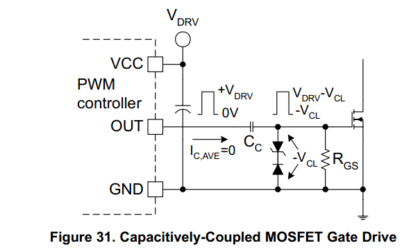
    I am reading slua618a , and have one more question on AC coupled gate-drvie of figure 31. Kind of confusion.

    I think for "mosfet gate is driven between -VCL and VDRV-VCL levels instead of 0V and VDRV" , there should be a hidden assumption that , the initial level of OUT pin is High(VDRV) and so the first PWM pulse starts with a falling-edge which changes from VDRV to 0. 

    (1)Suppose the system just powered on, PWM controller has not start to workyet, and the initial level of OUT pin is High(VDR) , so AC coupling cap Cc has VDRV on its left pin and 0V on its right pin. Then the first PWM pulse is falling-edge which changes from VDRV  to 0 on OUT pin,  this will cause a first falling edge on mosfet gate (Cc right terminal ), which would be 0--> -VDRV, but will immediately be Clamped by the Zener and Diode network, so mosfet gate would see a falling-edge of  0---> -VCL.  Consequently the following rising edge ouptut on OUT pin will cause a rising edge of "-VCL---> VDRV-VCL" on mosfet gate. the cycles go on, and the gate volatge is driven between -VCL---> VDRV-VCL as expected.

    (2) then Let's look at the opposite situation to the upmentioned assumption:  Suppose the system just powered on, PWM controller has not start to workyet, and the initial level of OUT pin is LOW (0V) , so AC coupling cap Cc has both 0V on its two terminals. Then the first PWM pulse is rising-edge which changes from 0  to VDRV, and this will cause a first rising edge on mosfet gate (Cc right terminal ) which is also 0-->VDRV, and consequently the following falling edge ouptut on OUT pin will cause a falling edge of "VDRV--->0V" on mosfet gate. the cycles go on, and mosfet gate is driven between 0 and VDRV, but there will be no -VCL anymore as the diodes network seems have no chance to work.

    Therefore, this seems impose some requirement on the intial level of OUT pin of PWM controller. Not sure whether my perception is correct or not. Would you give  some advice? Thank you very much.

  • Yi,

    great question!

    Situation (2) is probably the common situation, as in most cases from a powered-off state, both terminals of Cc would be same potential. Without presence of Rgs and ideal components, the effect you described would happen, but there is the RC time constant of Cc and Rgs that defines how long it takes to reach the DC level. Another way, Rgs pulls the current down to source, so the voltage will drop periodically. If you simulate this, you can see the start up time will take a long time to see the Vdrv-Vcl to -Vcl levels with a very large RGS value, and very short with low Rgs, but then the ripple will be very large.

    When the current falls thru Rgs, the voltage drops a bit, then the PWM falls, and the off-state voltage at gate approaches -VCL defined by the clamp. You would see the PWM signal DC voltage drop over time. This effect and calculation of the time constant is detailed in 6.2.

    http://www.ti.com/lit/ml/slua618a/slua618a.pdf#page=38

    The effect of time constant from Cc and Rgs is section 6.2 linked above. If Rgs is chosen lower, the Ripple will be higher, but startup time would be lower. Thats basically the tradeoff. 

    Hope this answers your question! Let me know by pressing the green button. And let us know if you have more questions.

    Best

    Dimitri