This thread has been locked.

If you have a related question, please click the "Ask a related question" button in the top right corner. The newly created question will be automatically linked to this question.

UCC21710-Q1: time delay before OC pin is activated

Part Number: UCC21710-Q1
Other Parts Discussed in Thread: UCC21710, UCC21732

Hi Ti engineers,

I have a question about time delay of OC-pin.

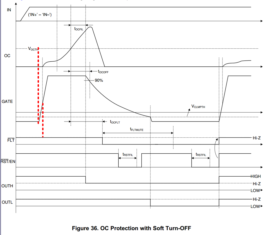
According to the datasheet, "The OC pin is in high-impedance state when the output is in high state, which means the overcurrent and short circuit protection feature only works when the power semiconductor is in on state."

I am wondering whether "OC pin becomes Hi-Z" and "output becomes high state" occur simultaneous or not? If "OC pin becomes Hi-Z" occurs after "output becomes high state" with some time delay, and then how much the time delay is?

Appreciate any information you can provide. Many thanks.

Zack


  • Hi, Zach,

    Welcome to e2e, and thanks for your interest in our products.

    Check out Figure 36, this shows how the over-current protection works. Figures 24 and 26 include timing information as well.

    Let us know if you have further questions.

  • Hi Don Dapkus,

    Many thanks for your reply. In fact, I was confused by the difference of datasheet figure and the simulation results.

    According to the datasheet, it seems that there is a tiny time delay to release oc pin after gate increases. In fact, I am not very clear about the meaning of "Gate" here. Is it the gate voltage across the gate-source terminals of the mosfets, or the voltage of OUTH/OUTL pins of this IC. Or maybe there is no big difference for them.

    However, according to the simulation results. there is a more than 250ns time delay, which is too large for my application. Please see the following picture.

    I used the UCC21710 Unencrypted PSPICE Transient Model provided by Ti and then converted it into LTspice simulation to get the below results. Is this 270ns time delay true for ucc21710?

    or is it possible for ucc21732 since there is 2L soft turn-off in the vgs waveforms, which is consistent with the characteristics of ucc21732.

    And another question about UCC21710 Unencrypted PSPICE Transient Model, why dose this model have the 2L soft turn-off characteristics of ucc21732? Is that right?

    Appreciate any help you can give. Many thanks.

    Bests,

    Zack

  • Hello Zack,

    There is no internal delay for the OC pin to begin rising. It is able to track the voltage applied to the pin within a few tens of nanoseconds of the OUTH pin going high. The Gate signal is denoting the actual voltage of the IGBT or SiC MOSFET. This is different than OUTH/OUTL when there is a gate resistor present. 

    The reason the figure shows a small delay between Gate going high and OC going high is representing the time before the Gate reaches the threshold voltage of the IGBT or SiC MOSFET. The current through the device will not begin to rise until this threshold is met. Thus, the OC voltage does not sense the current until the Gate voltage is high enough to allow current to flow (through the sense resistor or other means of connecting the OC pin). 

    Whatever is causing the delay in your simulation should not be due to the IC. Can you share a snapshot of the circuit?

    I do not see the 2LTO behavior in my simulation model. It is the STO behavior. It is hard to see from the waveform you share whether the turn-off exhibits STO or 2LTO behavior. Additionally, if you are simulating with a power device model, you may see a plateau voltage due to the power switch characteristics itself during STO, rather than a plateau voltage induced by the gate driver.

    Regards,

    Audrey

  • Hi Audrey,

    Many thanks for your quick reply. Now I am clear about timing question. Then let's focus on the simulation issues.

    First, here gives the circuit and simulation results of ucc21710 with VDD=15V. This is a single switch hard-switching short-circuit fault testing. The model of mosfet tested is from Wolfspeed.

    For the waveforms, the sequence follows:

    vds: drain-source voltage of mosfet; iL1 is the short circuit current.

    voc: the voltage on oc pin.

    vgs: gate-source voltage mosfet, vpwm_in: pwm signal input.

    Overall, the simulation results are strange, I think. When the fault is detected, vgs is still at high output for long time, which is even longer than the pwm signal. It is amazing.

    In order to illustrate the possible 2LTO, I increased the value of VDD, then you can notice the change of vgs during fault condition. It looks like the 2LTO.

    I also find another interesting thing about ucc21732. I just replace above ucc21710 LTpsice model with ucc21732 LTspice model and add the external mosfet for clamping function. The left circuits remains the same with the above ones (VDD=15V). 

    From ucc21732's results, vgs can be shut down normally, but there is no any 2LTO waveforms as datasheet mentions. It looks like that these two models swap their fault turn-off characteristics. For ucc21710 and ucc21732, I just used online unencrypted models, and converted them into LTspice to get simulations.

    Many thanks for your time and hep.

    Bests,

    Zack.

  • Hi Audrey,

    I just modified my simulation setup and then find something to clear some of my questions.

    I put the rest signals to clear fault signals and thus I can obtain the multiple and continuous short-circuit behaviors. I found that after the first two abnormal events, the vgs looks normal at the third pulse. You can see the following the pictures. The first picture is about ucc21710 and the second one is about ucc21732.

    For ucc21710, the vgs will be shunt down at the third fault pulse, which is different from the first two pulses. And there is no 2LTO for the normal waveforms.

    For ucc21732. the vgs will reobtain the 2LTO function at the third fault pulse, which is different from the first two pulses.

    So I guess the previous simulation may be related to the start-up process? Since it is just my guessing, I still want to get your comments and suggestions. Many thanks. Appreciate the discussion with you.

    Bests,

    Zack

  • Hello Zack,

    The VDD UVLO delay to Output High is 5us and the VCC UVLO delay to Output High is 37.8us. It does not look like UVLO startup delay since the output follows the input from the first pulse. This is unusual behavior and I will need some time to check the model and your circuit more closely.

    If you delay the start of the simulation (after 10us) does the behavior persists?

    Additionally, what is your command statement "ic. v(C1)=0"?

    Regards,

    Audrey

  • Hi Audrey,

    Sorry for the late response. Hope you are doing well recently.

    You are right. Just follow your suggestion, I delay the start of simulation by adding a delay for pwm output, but I am sure this is what you suggest me to do? Fortunately, there is no this strange phenomenon anymore. Please find the attached two picture, one is for ucc21710 and the other one is for ucc21732. 

    BTW, you can ignore "ic. v(C1)=0" since it is not used in the simulation and I forgot to delete it. In the updated simulation, I deleted them.

    Anyway, previous issue can be avoided by adding a delay for pwm output. Appreciate your time and patience.

    Bests,

    Zack

  • Hi Zack, 

    That is great to hear! I hope you will be able to get a good understanding of the device features from simulation, but I also recommend you closely read the datasheet descriptions and understand the specifications. The datasheet is the final word for how the device will operate in the real system. You can also easily evaluate the part by ordering one of the EVMs!

    Feel free to create another post if you have new questions.

    Regards,

    Audrey