This thread has been locked.

If you have a related question, please click the "Ask a related question" button in the top right corner. The newly created question will be automatically linked to this question.

I use the UCC28600 for QR flyback,but the efficiency is lower than i expect.

Other Parts Discussed in Thread: UCC28600

Hello,TI engineer,

 i use the UCC28600 for qr flyback ,but the efficiency is low ,my condition is :

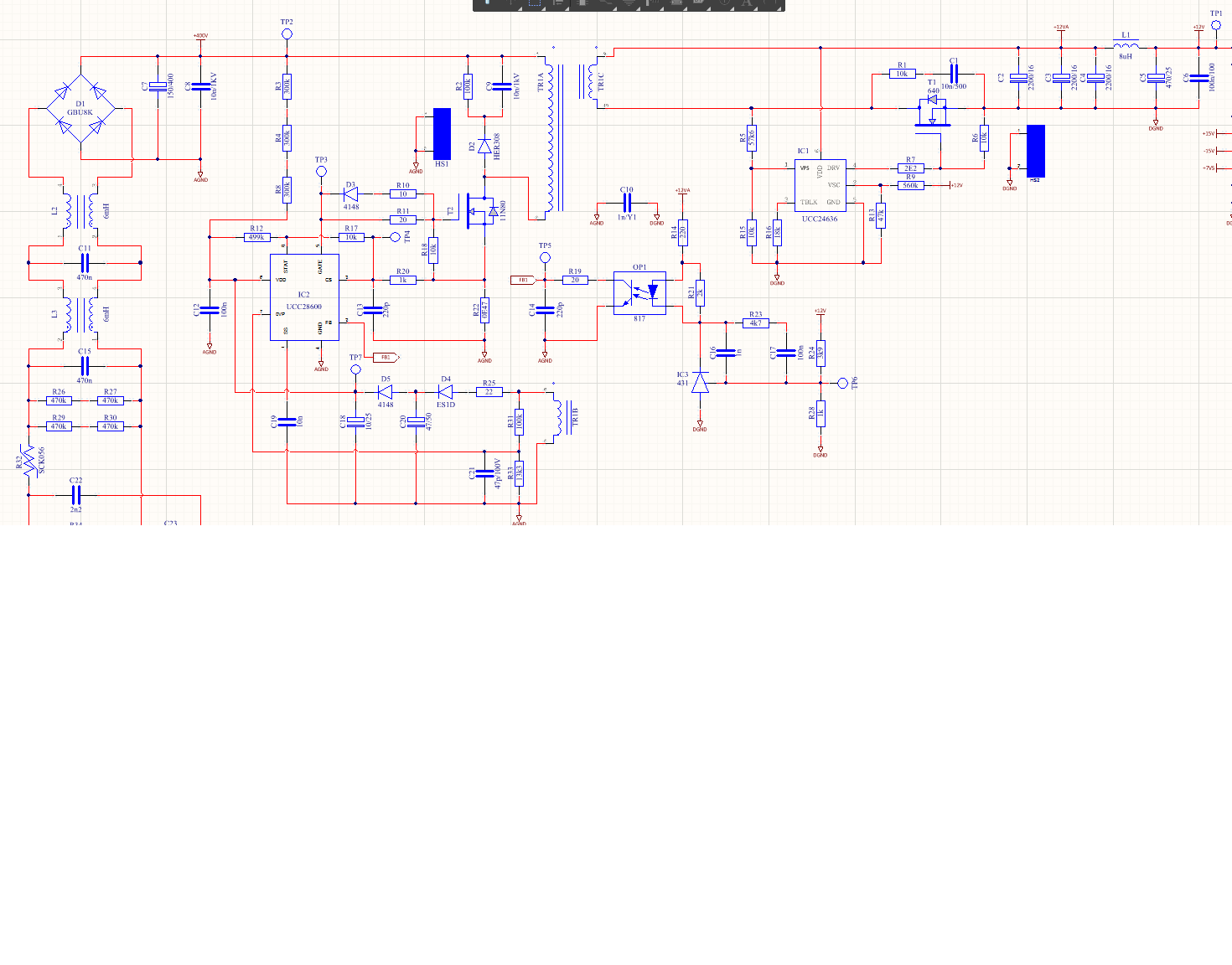
Input: 85Vac-164Vac, Output :12V 100W, the bias voltage is 12V also,

the transform design :PQ3230 NP=18 NS=2 Nb=2 Lm=100u Lk=3.5u 

schematic as below:

i do not use the SR and i place a diode (B20100G) temporary,the efficiency is about 78% at 5A ,and when to the full load ,the efficiency 75% .

the DS and GS  wave also as below:  i think the DS wave has bad ring,could you please help ?thanks

RCD i change to R=47K(3W) C=3N3 D=HER308 OR 4007,BUT not improve .

  • Hello User5865075,

    Thank you for your interest in the UCC28600 Flyback Controller.

    Normally, a 12-V, 100-W flyback converter should perform above 85%, which is ~17.6-W loss.  
    Your 75% full-load efficiency measurement indicates ~33.3-W loss.  This is about twice the normal loss, and any single component carrying most of the excess loss would be quite noticeably hot.  I recommend to check each power processing component for excessive temperature rise.  Investigate the one with the highest temperature first to determine why its loss is so high.  Then determine how to reduce that loss.  Then go on to the next hottest part, and so on.

    I agree that the Vds waveform is not very good, with too much high frequency ringing during the flyback interval (demagnetization).
    This is ringing of the leakage inductance with the MOSFET Coss capacitance.   Reverse recovery current from D2 instigates this ringing. The HER308 diode used in the RCD clamp is rated for 75ns reverse recovery time (trr).  But this trr gets longer when the junction heats up and allows the ringing to get worse. 
    Adding a damping resistance in series with the diode will help remove most or all of the ringing.  Please refer to this paper on RCD_R snubber design:
    RCD-R Damping Design.pdf

    I do not believe that this diode is the cause of the low efficiency.  I think it would fail with 17W+ power loss.  But I do think the low efficiency indirectly leads to higher peak primary current which heats up the snubber diode more than normal.  Check the transformer temperature.  If it is very hot, it probably needs to be redesigned.

    Regards,
    Ulrich

  • i scan the temperature of the board,only the RCD  and the output diode is hot.the others is lower than 50  degree.

    i  use the slow diode 4007(D2),it has no ring in it,but the leak voltage is too high,so i doubt the transform design,

    ,Do you think the transform parameter is correct for the power?

  • Hello User5865075,

    The slow diode may have additional forward recovery voltage drop that adds to the leakage spike voltage.

    The transformer parameters that you listed seem to be okay.  The peak primary current may be a bit high.

    I suggest that you fill out the UCC28600 Design Calculator tool http://www.ti.com/lit/zip/slvc104 to make sure you are using the correct parameters for your design targets, including the current sense resistance and other programming components around the controller.   

    To measure temperature of the transformer, you'll need to run the converter at full load for 30 minutes or more to allow the mass of the transformer to settle at its steady-state temperature.   For any change in input or output conditions, give it plenty of time to settle to the new temperature.

    Regards,
    Ulrich