This thread has been locked.

If you have a related question, please click the "Ask a related question" button in the top right corner. The newly created question will be automatically linked to this question.

UCC27714: HB-HS voltage drops when UCC27714 top temperature reaches 70C

Part Number: UCC27714

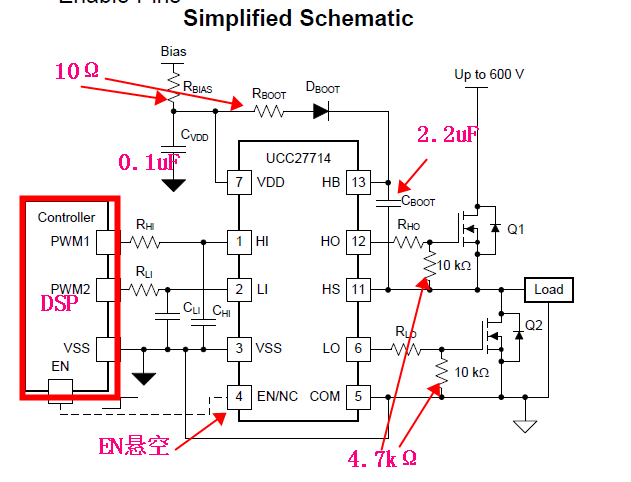
Hi, my customer's schematic is as below(EN floating).

We find that when UCC27714's top temperature reaches 70C, the HB-HS voltage will drop to below 7V, causing UCC27714 to restart repeatedly.

The waveforms are as below:

yellow- good bootstrap cap voltage waveform(UCC27714 whose temperature is less than 70C)

blue- good HO-HS voltage waveform

green- bad bootstrap cap voltage waveform(UCC27714 whose temperature is above 70C)

red- bad HO-HS voltage waveform

The device power supply is stable, and we've tried to replace the device and the problem is still there. Within the same device, if we cool down the temperature to below 70C, the problem disappear.

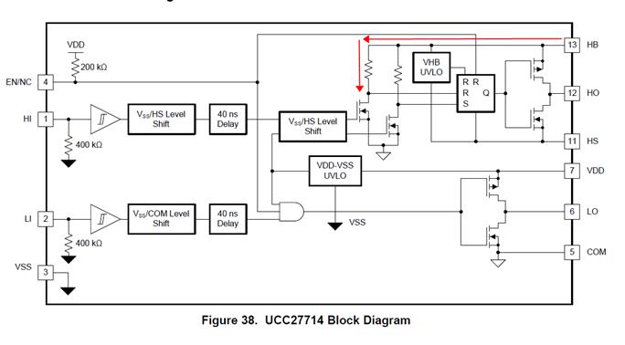
Are there any internal circuit that could discharge the bootstrap capacitor during high temperature? For example the red line shown below?

Are there any risk for the schematic we provide?

  • Hello Howard,

    Thank you for supporting the UCC27714.

    I have some comments to confirm. To determine the junction temperature of the UCC27714 we need to know the power dissipation so we can determine the device top to junction temperature difference.

    To determine this please provide: VDD voltage, switching frequency, Mosfet part number and # devices in parallel (if applicable) , and the gate resistance from the gate driver to MOSFET gate.

    We usually recommend the VDD cap value of 10x the HB-HS capacitance to reduce the VDD voltage drop from HB cap charging. Can you confirm if there is additional capacitance on VDD beyond the 0.1uF shown?

    Can you provide the part number of the boot diode? We would recommend a fast recovery diode to reduce the possible HB cap discharge during the boot diode reverse recovery time.

    Even when the switching stops, the green waveform looks much lower during the high temp example than the "good waveform". Is the yellow and green waveforms ground reference the same, and same voltage scale?

    The 10 ohm resistance in series with the boot diode, and 2.2uF boot capacitance is a long time constant. Can you confirm if reducing the resistance to 2.2-4.7 Ohms may help the operation?

    Confirm if this addresses your questions, or you can post additional questions on this thread.

    Regards,

  • 1. we've decreased Rboot to 1.1ohm but it doesn't help.

    2. Dboot is STTH110A

    3. 70C is measured by thermocoupler attached to the top of the IC. VDD is +12V, switching frequency 60kHz, single MOSFET IRF300P226(NO Parallel). Gate drive resistor is 10ohm. Maximum duty cycle is 90%.

  • Hello Howard,

    Thank you for the update and the application operating details. I would like to review the HB cap and power dissipation. Referring to the UCC27714 datasheet section 9.2 the recommended boot cap minimum value is determined by estimating the equivalent Cg from Qg/Vgs, or 191nC(max)/11.3V=16.9nF. The boot cap is recommended to be 10x the Cg which will be 169nF. The 2.2uF is much larger than required. We do always recommend margin on the boot cap value, but 470nF should be adequate for this application. Does the converter operation have conditions where the Fsw is low, or the HO on time is long.

    The total gate drive power is 2 x Qg x VDD x Fsw, or 2 x 12 x 127nC(typ) x 60kHz=182mW. With the external gate resistance not all of the power is dissipated in the driver, but even with 182mW and a IC top measurement of 70 deg, the difference of the top and junction will only be 0.182 x 3.6 degC/W or 0.65 deg C. The 3.6 degC/W is the junction to top characterization parameter.

    It does not appear that the junction temperature should be close to the max operating range.

    I would try a boot capacitance of 0.47uF X7R ceramic which will allow the boot cap to charge/recharge faster than the 2.2uF. Is the 2.2uF a ceramic capacitor, or other type?

    The STTH110A voltage rating seems higher than needed for the application, the forward recovery time seems long at 300ns. Can you try a 600V rated diode such as the MUR160 which will have faster switching times?

    If the boot diode and HB capacitor change does not help, it is possible there is a change in the behavior at this temperature that causes an issue. If the UCC27714 has excessive HO overshoot or undershoot it is possible the output may not maintain the correct state. If this is a possibility, we recommend adding schottky diodes on the driver output (HO in this case) to clamp to the bias and driver ground reference. Place the diodes, 1A rated, close to the IC pins from HO to HB and HO to HS to limit the positive and/or negative overshoot/undershoot.

    Confirm if this addresses your issue, or you can post additional questions on this thread.

    Regards,

  • Richard,

    thank you.

    They changed the VDD cap to 4.7uF, and boot cap to 0.47uF and the problem solved.

    But still curious why it can solve the problem. We have measured the waveform with original cap value when HB-HS voltage will drop, the VDD voltage is very stable as shown below purple line

  • Hello Howard,

    It is good news that the changes resolved the issue. It is not clear exactly why this is happening,. The 4.7K resistance on the Vgs will result in more current draw than the IC HB should have. The temperature of the IC junction we confirmed should not be an issue.

    One possibility that may change behavior at temperature is the boot diode behavior, maybe longer recovery or high leakage.

    If you want to confirm what may be happening, if there is a way to measure the current to the driver IC (IDD) by itself (no shared other load) you can check over temperature to see if there is any increase at high temps.

    Confirm if this addresses the issue, or you can post additional questions on this thread.

    Regards,

  • Richard,

    Why we emphasize that VDD cap should be at least 10 times of boot cap? 

    My understanding is that the purpose is to keep VDD stable when charging boot cap, but VDD is already stable even with the original cap value.

    All the other suspects you mentioned like higher leakage at higher temperature, if it's the case, it's still there. Why changing the cap value would solve the suspected problem?

  • Hi, Howard,

    Ni hao! Let me jump in here.

    We specify VDD cap >10X of boot cap to make sure the VDD supply is stable to the IC. Remember the inductances in the system, so depending on where VDD was measured, you may not see the true story. And, you can't actually measure the VDD on the die itself. There is a drop across the internal inductance of the bondwires. So, what you measure externally is not what the die itself actually sees. And, if you don't measure the voltage with proper techniques, you may not get the full story. You need to measure as close to the IC as possible to get an accurate measurement.

    For the same reason, it is critical that the decoupling capacitors be placed extremely close to the IC itself. Again, you want to minimize the parasitic inductance of the trace.

    If you want more details, I have a presentation I can email you that we did a while ago that illustrates this concept.

  • Don,

    thank you, please email me the presentation.

    In the last post i said"They changed the VDD cap to 4.7uF, and boot cap to 0.47uF and the problem solved."

    In fact, They have tried CVDD=0.1uF, and boot cap to 0.47uF, and it also works.

    But if they use CVDD=0.1uF, Cboot=0.22uF, the device won't pass HI to HO at the startup.

    So it seems that only Cboot is determine whether the circuit could work or not, it's not a must that CVDD to be 10times larger than CBOOT.

    Why too large or too small boot capacitor will result in abnormal working?

  • Hello Howard,

    I sent the presentation or app note on selecting boot strap components for half bridge drivers to your email.

    the link is also here:

    You want to size the boot capacitance with a large enough value to be able to charge the MOSFET Qg without excessive voltage drop on the HB bias. If you size the boot cap too large there are tradeoffs in being able to charge the boot capacitance relatively fast during the LO on time initial cycles.

    Regards,