This thread has been locked.

If you have a related question, please click the "Ask a related question" button in the top right corner. The newly created question will be automatically linked to this question.

UCC21520: PMSM Driver Phase Voltage Ringing

Part Number: UCC21520
Other Parts Discussed in Thread: UCC21540A

I have designed a PMSM controller, everything is working fine.

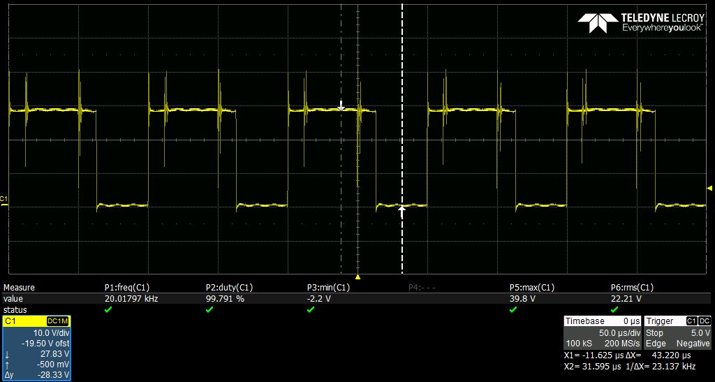
But at phase voltages, there are some ringings.

What can cause to this problem?

Mosfet drivers UCC21520 parallel 2 channel for each mosfets, i am driving all mosfets with discrete mosfet drivers with isolated 12V DC-DC converter.

I have increased and decreased gate resistors to 0R-10R range, nothing changed.

I have also RCD snubbers, 1R+47nF capacitors to mosfets.

Fsw=10kHz

Bus voltage is very smooth, no ringing. Bus capacitors are 5x6800uF Al-El Capacitors and 20x22uF ceramic capacitors.

At 100 rpm there is not ringing at phase voltages, ringing is increasing by motor speed increase. Phase current around 15A.

Mosfets has large Qgs 375nC, 2 parallel mosfets.

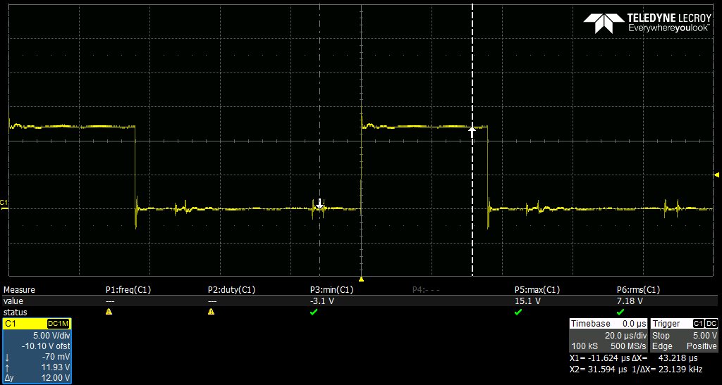
this is low side Vgs voltage, small ringing can seen in the gate voltage, but at high side there is no ringing.

  • Hi,

    Welcome to e2e, and thanks for your question.

    It looks like this may be a measurement artifact. How are you measuring the signals?

    Please see Figure 6 of this document for a method to reduce the loop inductance of the measurement loop to minimize noise pickup: http://www.ti.com/lit/ug/snou150b/snou150b.pdf

    I assume the spikes line up with the switching of another mosfet in your system? I am assuming you are just picking up noise from those switching events in your measurement.

  • Hi,

    Thanks for fast answer.

    I am measuring with ground spring clip so i think it is not measuring error.

    May it be self turn on phenomenon?

    The spikes are 2.2Mhz frequency.

    Thanks.

  • Hi,

    Thanks for fast answer.

    I am measuring with ground spring clip so i think it is not measuring error.

    May it be self turn on phenomenon?

    The spikes are 2.2Mhz frequency.

    Thanks.

  • Hi,

    It could be. Do you have an RC low-pass filter on the input? Have you scoped the inputs to see if this noise is coupling thru the inputs?

    Another potential cause could be noise coupled onto the DT pin. Do you have it hard tied to a supply, or decoupled with a capacitor to reduce noise? See section 8.4.2 Programmable Dead Time (DT) Pin of the data sheet for more information on best practices for the DT pin.

  • At the PWM inputs, there is 49R9 + 470pF RC network.

    I have pulled up DT input to 3V3 supply.

    I have changed deadtime using software 200ns-4us range, nothing changed.

    I am attaching mosfet driver and phase power stage. I am using all high side and low side mosfets to same mosfet driver circuit, all have discrete 12V isolated DC-DC converter to supply.

  • Hello, Thanks very much for the information.

    I reviewed the waveform, and it looks the noise is highly possible introduced from cross coupling from Cgd, which is big in your system.

    Installing Typically larger Rg or a 30Ω to 100Ω at 100MHz ferrite bead will ensure clean operation.

    I would suggest you may replace R27 and R35 with a around ~100Ω@100MHz, and you should see improvements.

    Let us know your thought.

    Wei

  • Please let us know if you have any updates, Thanks.

  • Hello, thanks.

    I have tried so many things.

    I used 100ohm @100mhz ferrite bead on as you mentioned in R27 and R35, it did not change anything. My gate signals are clean actually.

    I replaced gate resistors in 4.7R-27R range, it did not change anything also.

    I put a parallel 4R7 on snubber resistance, this lowered peak voltages.

    I changed snubber capacitors to 200nF, this lowered peak voltages.

    I also soldered high ripple current 12uF film capacitor to dc bus, it does not also changed anything.

    But peaks can be reached to 45V at 28VDC supply. 

    The mosfet i am using is VS-FC420SA10. It has quite parasitics. And maybe my layout has some parasitics.

    Reverse recovery diode charge is quite high, i soldered anti parallel diodes every mosfet, peaks get a bit higher.

  • I have one idea and I believe it will make a difference.

    Change the driver voltage from 12V to 10V with UCC21520, or 8V with UCC21540A, you will see ringing reduction. For MOSFET, you have barely little benefit to drive over 10V, instead you will see much noise.

  • Hello.

    I am using DC-DC converters to supply mosfet drivers, so i can not change them to 10V.

    But i guess problem is caused by layout.

    Ceramic capacitors's return path and motor drive current return path are different and capacitor path is more long.

    I soldered every half bridge leg's + and - film capacitor, ripples decreased. But i still see some ripple on phase voltages.

    I think i need to redo layout design and be careful about decoupling capacitors.

  • Thanks very much for the information. Good luck with the layout. and let us know if there is any help from our side. A few mindful points in regarding to layout.

    1. Power loop - halbridge transistor and bypassing capacitor, may consider vertical loop in stead of lateral loop.

    2. Gate driver loop - especially minimize the common source inductance

    3. switch node - minimize the overlap which is close to switch node, since switch node is the noise source.

    Best regards,

    Wei

  • Thanks for reply.

    I want to ask some questions about layout.

    Mosfets are quite large,so current loops are become long.

    For decoupling capacitors and return current, is it okay to use ground plane and power plane all over the PCB?

    Switch node is a noise source, i am not sure about to put ground plane and power plane below switch node?

    I can use film capacitors to decoupling but what should i choose them for ripple current value? Should i choose the film capacitors for ringing frequency or PWM frequency? Should i choose the film capacitors for minimum impedance frequency value?

    Mosfet drivers are located in another PCB, for 10kHz PWM frequency should i locate them in mosfet power board and close to mosfets?

    Due to very large inrush current of capacitor's, what can you suggest to control inrush currents?

    Thanks.

  • Thanks, and I saw the datasheet of the MOSFET and yes, it is big in size.

    for capacitor in the bus positive and negative rail which doesn't switch, it is perfectly fine to use pcb layer planes to create capacitance, which is helpful.

    Switch node has some trade off, you will try to avoid overlap as much as you can since it is switching.

    Film cap and ceramic cap are good for high frequency decoupling, especially multi layer ceramic caps.

    Yes, it is better to put the driver as close as possible.

    For inrush current, maybe modeling it into a simulation tool will give you more guidance.

    Good luck.

    Wei