This thread has been locked.

If you have a related question, please click the "Ask a related question" button in the top right corner. The newly created question will be automatically linked to this question.

TPS43060: Power management forum

Part Number: TPS43060
Other Parts Discussed in Thread: CSD18543Q3A, TPS43061

Hi,

I've developed a circuit to boost the input from 12V to 30 V using TPS43060 (I did use Ti WebBench for that).

The problem is that there is not switching frequency generated form the device, therefore, It cannot drive the gates of the two Fets (CSD18543Q3A). I've built three different circuits to compare but they have the same problem; no switching frequency. I've also followed the configuration from the evaluation board but there was no difference, and there was 7.5V at PGOOD pin.

What could be the sources of the problem?

Thanks in advance.

Regards,

Nghia

  • Dear Sir,

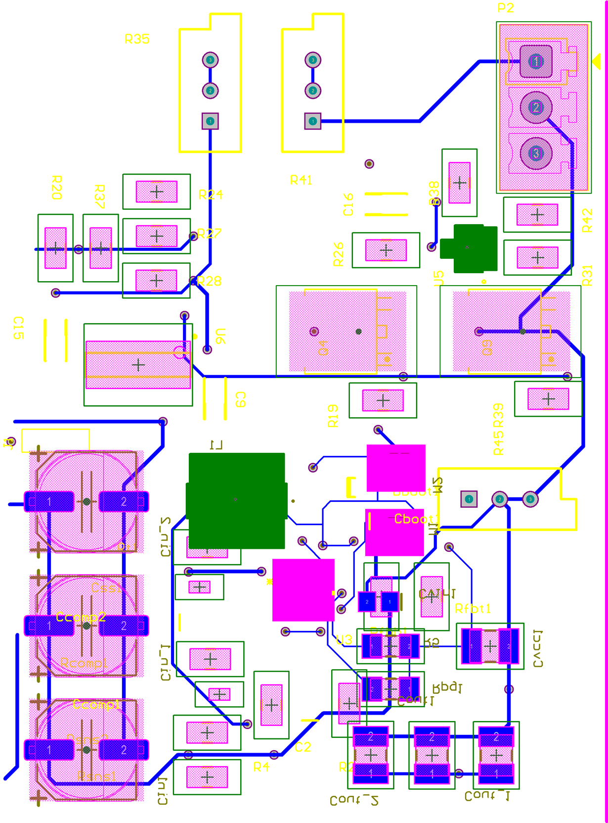
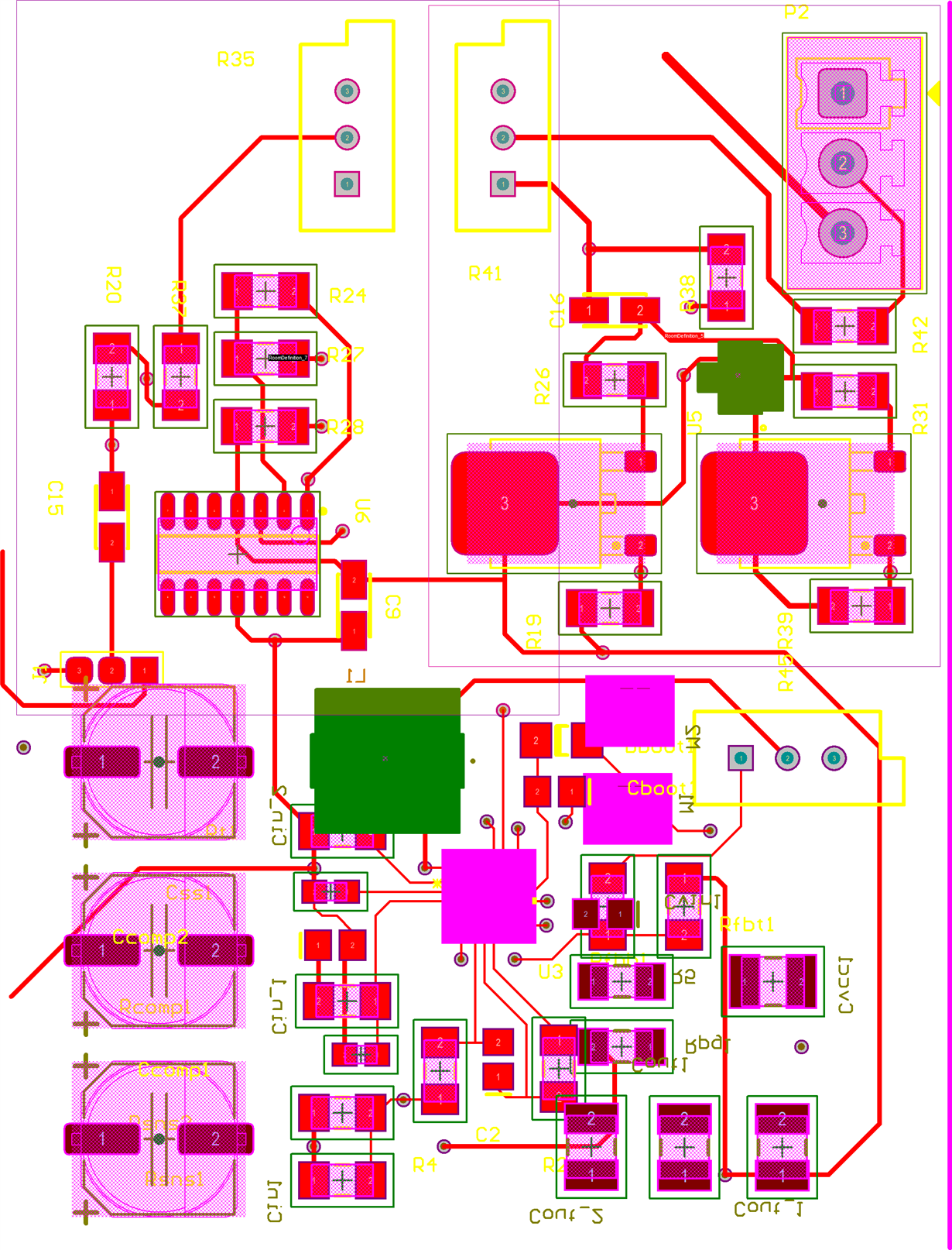
    Could u please share your schematic and pcb layout with us?

  • Hi Helen,

    Thanks for your response.

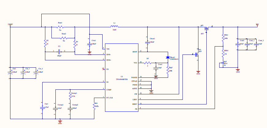
    Attached are the circuit diagram and PCB outline. All the connections are as in the drawing on the circuit boards. Should I see the clock signal on pin-1 and switching signal at gate driver pins?

    The original  circuit generated from Ti WebBench. But I can see it is not much different from the the evaluation board's circuit.

    Thanks & regards,

    Nghia

  • Dear Sir,

    Thanks for sharing the schematic with us. From the schematic, I found the EN pin is open, no connection. The EN pin is to enable IC to working. It should be pulled high to Vin to make the TPS43060 start working.

  • Hi Helen,

    Thanks for your supports.

    I did not connect the EN pin due to refer to the the original design from Ti Website and also the device's datasheet (on [page 3): "

    Enable pin with internal pullup current source. Floating this pin will enable the IC. Pull below 1.2 V to enter low
    current standby mode. Pull below 0.4 V to enter shutdown mode. The EN pin can be used to implement adjustable
    UVLO using two resistors." I will try anyway and let you know.

    Thanks & regards,

    Nghia

  • Hi Helen,

    No luck, I've connected 12V to pin 15 (EN), but nothing has changed. I believed the EN pin has internal pull-up so we can just leave it open if there is no need to control it.

    Regardless of how you put the component values, there must be clock or switching signals at different frequency? What else can we try?

    Thanks & regards,

    Nghia

  • Hi Nghia,

    Please send the source layout file to me. TPS43060 is a little bit sensitive to the layout. Please tell me what kind of layout tool you used? AD, Cadnece... or something else so that I can open it in the related tool.

  • Please take the TPS43061 EVM board for a reference at the same time to save time.  Please also refer to the layout guideline and layout example on the datasheet for a check..

    I will check your layout file once I get your file.

    By the way, what is your maximum load current and what kind of Boot diode your chosen. could you please share the datasheet of the boot diode with us?

  • Hi Helen,

    I've ordered the EVM board. Will let you know if I could find something that causes the problem.

    The boost diode is the CDBW46-G ( SCHOTTKY 100V 150MA, recommended from the schematic generated from Ti WebBench). As you can see from the schematic, I've tried to keep everything exactly as the WebBench's generated schematic.

    Thanks & regards,

    Nghia

  • Thanks for the update.

    I'll check the spec of the CDBW46-G tomorrow(generally for the boot diode, Schottky is not recommended because of the big leakage current). I'm very very busy today.