This thread has been locked.

If you have a related question, please click the "Ask a related question" button in the top right corner. The newly created question will be automatically linked to this question.

UCC28950: the value of Rab

Part Number: UCC28950

Dear all,

I would like to ask about Rab of UCC28950.

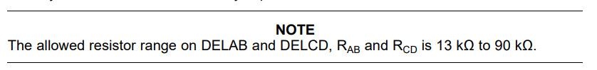
The following was mentioned in the data sheet.

I would like to answer the following questions.

(1) How did you decide the range of Rab and Rcd described above?

(2) Our customers try to set Rab between 8.2kΩ and 10kΩ to minimize the dead time of OUTA and OUTB.
If Rab is set to a value smaller than 13 kΩ, what kind of adverse effects may occur?

Best Regards,

Y.Ottey

  • Hello

    The lower limit was set at the time that the part was designed. The limit of 13k was set by considering the long term reliability of the IC. The upper limit was set by considerations of noise sensitivity. TI will not recommend operation outside these limits.

    Attached is a document that describes how the ADEL and ADELEF pins may be used to set fixed delays which are shorter than those that can be achieved with a 13k resistor at DELAB and DELCD pins.

    /cfs-file/__key/communityserver-discussions-components-files/196/1462.Calculating-Adaptive-Delays.pdf

    Please let me know if you need further information.

    Regards

    Colin

  • Dear Colin

    Thank you for your reply.

    I would like to ask adding question about your answer.

     The limit of 13k was set by considering the long term reliability of the IC.

    If the resistance is lower than 13kΩ (8.2 to 10kΩ) for a long period of time, can it be recognized that the operation is unstable or the performance as the data sheet cannot be obtained?

    Regards,

    Y.Ottey

  • Hello

    The minimum recommended resistance at DELAB and DELCD pins is 13k. The controller will produce shorter delay times if you use resistors less than 13k and these delays should be stable so this practice would be acceptable in a Laboratory environment. I would expect that the controller would operate for weeks with these lower resistances without problems BUT as I said, the long term reliability will be compromised. If you find that you need 10k to produce the delays you want then that is ok for short term lab testing and the correct long term solution is to set the resistors to 13k and use resistors at the ADEL and ADELEF pins to shorten the delays as described in the document I posted earlier.

    Regards

    Colin

  • Dear Colin

    Thank you for your reply.

    " I would expect that the controller would operate for weeks with these lower resistances without problems BUT as I said, the long term reliability will be compromised."

    Is the factor that impairs long-term reliability when Rab is 13 kΩ or less due to a shorter dead time?

    ”the correct long term solution is to set the resistors to 13k and use resistors at the ADEL and ADELEF pins to shorten the delays as described in the document I posted earlier”

    If the cause of impaired long-term reliability is shortened dead time, why is fixing the Rab to 13kΩ and changing Ka and CS to reduce the dead time is the correct long term solution?

    Regards,

    Y.Ottey

  • Hi

    I can't really discuss the reasons for the impairment of the long term reliability other than to repeat what I've already said - sorry.

    Separate circuits are used to effect the Adaptive Delay times. This means that the stresses on the circuits used to set the the baseline delays at DELAB, DELCD and DELEF are not changed even though the delays are shortened.

    Regards

    Colin

  • Dear Colin

    Thank you for your reply.

    I understand about your answer.

    I would like to ask a question.

    ”the correct long term solution is to set the resistors to 13k and use resistors at the ADEL and ADELEF pins to shorten the delays as described in the document I posted earlier”

    We got the following information from our customers:

    • Use CS-voltage at almost 0V
    • If you try to change the voltage value of CS by biasing the CS pin separately, the control characteristics will change.

    Although it looks like the above state, is there any other way than fixing the Rab to 13kΩ and changing Ka and CS to reduce the dead time?

    Regards,

    Y.Ottey

  • Hello

    I'm really afraid that I don't understand your question - sorry.

    If the CS voltage is almost zero then they won't have PCM  or over current protection (If in current mode control) or over current protection if using Voltage mode control.

    The control loop characteristics should not change as CS pin voltage changes unless the system has reached some internal limit (Dmax for example) and ceased to behave as a linear system.

    If they want to reduce the dead time then they should fix Rab at 13k and then use a potential divider from REV to GND to put a DC voltage on the ADEL pin - I believe this method was included in the .pdf file linked earlier in this thread.

    Please feel free to post their schematic and details of what dead time they want to achieve - if they don't want to post it to this public forum then you can send it to me directly at colingillmor@ti.com

    Regards

    Colin

  • Dear Colin

    Thank you for your reply.

    I understand other way to reduce TABSET.

    ”If they want to reduce the dead time then they should fix Rab at 13k and then use a potential divider from REV to GND to put a DC voltage on the ADEL pin-I believe this method was included in the .pdf file linked earlier in this thread.”

    I also checked the contents of the PDF file I received from you.
    I would like to answer the following questions.
    1. When applying a fixed voltage to the ADEL pin, is it acceptable to recognize that the control characteristics do not change if the ADEL pin voltage is in the range of 0 to 2V, similar to the CS pin?

    2. When applying a fixed voltage to the ADEL pin, we assume that the CS pin is not connected to the ADEL pin. At this time, is it okay to recognize that the dead time does not change if the CS pin voltage changes?

    Regards,

    Y.Ottey

  • Hello

    1/ The voltage at the ADEL pin will not affect the control characteristics of the system.

    2/ Correct - the ADEL pin is connected to a fixed voltage and there is no connection from ADEL to CS then the CS voltage will have no affect on the dead time.

    Regards

    Colin

  • Dear Colin

    Thank you for your reply.

    I understand about your answer.

    I would like to ask a question about CS pin.

    "The control loop characteristics should not change as CS pin voltage changes unless the system has reached some internal limit (Dmax for example) and ceased to behave as a linear system."

    As mentioned above, the control characteristic does not change even if the voltage is changed by externally biasing the CS pin (unless the internal limit is reached).

    However, even if the CS pin is biased, the control characteristic is changed. Is the reason why doesn't change?
    Since the CS pin has the function of Current Sense, I think that it is a part related to the control characteristics of the device, so I speculate that it has some influence on the control characteristics.

    Regards,

    Y.Ottey


  • Dear Colin

    In addition to the previous post, I would like to ask additional questions.
    We have received a request from our customers to make only TABSET smaller. (TCDSET, TAFSET, TBFSET are not changed.)

    With the method you introduced, I think that changing the voltage on the ADEL pin changes not only TABSET but also TCDSET.

    Is there no way to shorten TABSET without changing TCDSET, TAFSET, TBFSET?

    Regards,

    Y.Ottey

  • Hello

    The resistors at the DELEF and ADELEF pins set the delays for the SRs (OUTE and OUTF) independently of the primary side delays set by the resistors at the DELAB, DELCD and ADEL pins.

    Yes, changing the voltage at the ADEL pin modifies both the AB and CD delays however the baseline delays can be set independently using the resistors at the DELAB and DELCD pins.

    So - let's suppose that the customer wants to set a 100ns delay at AB and 250ns at CD.

    A 13k resistor at DELAB sets the 250ns minimum AB delay and you can then apply a fixed voltage of about 250mV to reduce the AB delay to 100nS. So 250mV shortens the AB delay to about 40% of the initial baseline value and it will shorten the CD delay by the same proportion. To get a CD delay of 250ns then you would have to set a baseline delay of 625ns using the resistor at DELCD.

    Here's a document that shows how this and other calculations can be done - (I may have posted this earlier but here it is in any case) /cfs-file/__key/communityserver-discussions-components-files/196/3808.Calculating-Adaptive-Delays.pdf 

    Regards

    Colin

  • Hello

    The control loop characteristic is set by the topology (buck derived) and the various elements of the control loop - gains, transfer functions and so on. PROVIDED that the system remains linear the control loop characteristics will not change - the exception being that if the characteristic will change if the output inductor changes from continuous conduction to dis-continuous conduction.

    Given that you are operating the controller in Peak Current Control mode then the CS signal is used to set the operating point of the power stage - mainly the current delivered to the output and the duty cycle. IF you add a DC offset to the CS signal - there are at least two things to be VERY careful about

    1/ adding an offset will reduce the linear control range of the system - in particular you can expect the current limit point to be reached at a lower current with the offset in place.

    2/ the rate of change of the offset voltage must be lower than the loop bandwidth - ideally at least a decade lower - otherwise the offset will 'look like' a valid variation in the power stage current and the controller won't be able to regulate it out.

    Normally - it is not necessary to add an offset to the CS signal.

    Regards

    Colin

  • Hello

    My apologies for the delay in responding.

    If you put a DC bias on the CS pin then the control characteristics will not change because the error amplifier will compensate for the offset and the loop dynamics, gain, phase, won't be affected. There are a number of cautions I should apply to this

    1/ I assume that the error amplifier has enough control authority to make the adjustment so that it remains in its linear range.

    2/ If you add a DC bias to the CS pin then the current limit point will reduce because of the fixed 2V limit in the UCC28950 device - this could be compensated for by changing the CS signal scaling of course.

    This is all somewhat theoretical because in practice one would not add a DC bias to the CS signal.

    Regards

    Colin