This thread has been locked.

If you have a related question, please click the "Ask a related question" button in the top right corner. The newly created question will be automatically linked to this question.

UCC5390: PCB inquiry

Part Number: UCC5390

Hi,

my customer is using UCC5390 to drive SiCFET, there will be very small probability that UCC5390 will output high when input is low, and causing SiCFET false turn on, and they see the requirement below:

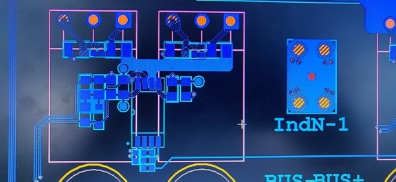
But they haven't followed the requirement, UCC5390 is placed on the first layer shown below:

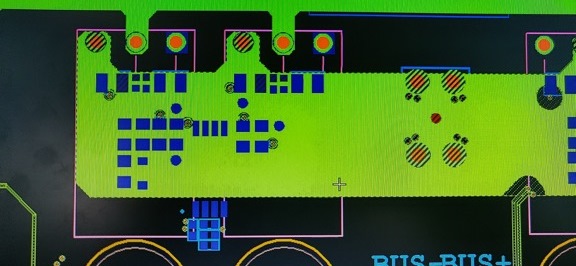
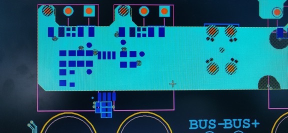
On the third and fourth layer, their will be plane under UCC5390. And there will be current and voltage variation on these 2 planes, dv/dt=43V/ns, di/dt=5A/ns.

They wonder what kind of influence it will bring to the gate driver, may it be the cause of the small probability that UCC5390 that give false high output?

Third layer

Fourth layer

  • Hi Howard,

    Thank you for your question. I work on the applications team in the high power drivers group.


    I'm going to pass this question along to someone who can provide more insight on this layout. I'll give you an update tomorrow on when I expect to be able to give you an answer.


    Thank you and best regards,
    Zachary

  • Zachary,

    thank you.

    Beside the question above, we would also like to know:

    1. Will "Barrier capacitance, input to output" become larger when the temperature rises? Since "Isolation resistance, input to output" decrease at high temperature. What can we know from this parameter?

    2. Will CMTI decrease when temperature rises? I know we can guarantee CMTI>100kV/us at full temperature range. 

  • Hi, Howard,

    Let's move this conversation to email. Can you mark this thread resolved?

    Back to the original question: why do we tell people not to put traces under the part... This is not because it has negative effects on our device, this is because it reduces your effective creepage and clearance distances, thereby reducing the effectiveness of the isolation. This is critical for applications that require reinforced isolation for safety applications. I don't think this is the case for your situation, so it should be ok, but I would recommend the customer fixes this in their next board revision to follow high-voltage best practices.

  • Don,

    This is not because it has negative effects on our device, this is because it reduces your effective creepage and clearance distances, thereby reducing the effectiveness of the isolation.

    I don't understand, my knowledge is that creepage and clearance is only related to the copper on the first layer. Will the copper on the other layer also affect it? Do you have any material to help me understand it? Thanks.

    Besides, it would be great if you could share some material to help me understand the parameter "isolation barrier capacitance" I asked in the same thread yesterday, I've no idea how it will affect the behavior of the device and whether it's affected by temperature.

  • Hi Howard, 

    In regard to the false turn-on, it is definitely not a good practice putting trace under the part in stead of the recommended layout, and it is very hard to quantify the risk.

    How about the 2nd Layer? what is the detailed information on layer 2.

    Let me know your thought.

    Wei

  • Wei,

    according to the file I searched online, creepage measures the shortest distance along the surface of the insulation material between conductors on a PCB. 

    So my understanding, if correct, creepage is only between two copper on the same layer(top layer and bottom layer) of the PCB, it's not between the copper on different layers. 

    And arc should be related to clearance since it's breakdown of the air, not creepage.

    Please correct me if I'm wrong.

    https://resources.altium.com/p/high-voltage-pcb-design-creepage-and-clearance-distance

  • Howard,  your understanding is correct. I had some bad experience of PCB internal arcing which lead me to think it about creepage.

    Going back to the coupling, it is quite difficult to quantify this coupling and false turn-on in this scenario. Do you know any reason why customer do it like this way?

    Wei.

  • Wei,

    thank you.

    The customer doesn't do it on purpose. They just want the copper plane to be intact and large and have already drawn the PCB in this way and make some whole product.

    That's why they ask why do we suggest no copper under UCC5390, it seems that isolation(creepage/clearance) is not the reason, then why do we suggest so? 

  • Hi Howard,

    If they are still on the stage of PCB layout, we recommend to fix the PCB.

    If they have already fabricated the PCB, they may go ahead the debug and measure the behavior of our driver.

    We don't have data on measuring the noise coupled to the input with copper below the driver. All the data taken is on the EVM or similar without any copper.

    What is on layer 2 Btw?

    Thanks.

  • Wei,

    there is no copper on layer 2.

    Then we recommend no copper under UCC5390 is because the noise may be coupled to the input of UCC5390, right? But we don't have any statistic, it's just in theory, right?

    We also observed that the false turn on probability rises at high temperature.

  • Yes, Howard, This is my best understanding.