This thread has been locked.

If you have a related question, please click the "Ask a related question" button in the top right corner. The newly created question will be automatically linked to this question.

TPS65150-Q1: Tps65150 does not have normal VGH output

Part Number: TPS65150-Q1
Other Parts Discussed in Thread: TPS65150

HI 

Now, tps65150 is used as LCD driver's high and low voltage. It needs + 18V and - 9.6V high and low voltage. In the following two problems (refer to the design below), please provide technical support. Thank you!

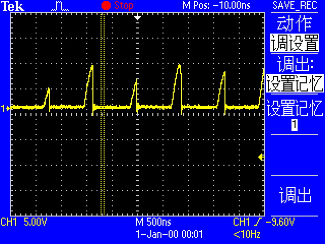
1. At the moment of power on (about 40ms), there is a normal switching frequency, and then there is no switching frequency, vs = VIN;

2. After changing the 100nF of the string between fdly and VIN to 0 ohm resistance, the 1.2M switch frequency is normal, the output is normal on VGL, and the 1.2MHz superposition level is normal on DRVN, but only 9.6V on VGL, and no output is available on DRVP,There is no action on the DRVP,Why is there no normal 1.2MHz stack level on DRVP,

3.I changed another application. I connected SW directly to the third pin of D20 without drvp voltage doubling. At this time, there can be 23v voltage on CPI, but VGH still has no output. I checked that the level of other pins in IC is vdly2 = 0V, vadj = 0V. What is the specific reason for this?

  • Hi, 

    I have notified our expert regarding this topic. Please expect a response by 5/28/20.

    Thanks,

    Aaron

  • Hi,

    Today, I did another verification, put the dly2 pin directly at 5V (VIN) high level, at this time, drvp has corresponding waveform output (as shown in the figure below), and VGH has 18V output, but this premise is to turn off fdly error detection, and directly connect 0 ohm resistance (as shown in the figure).

    1. Why does drvp output this waveform when my sample connects dly2 to 5V (VIN) high power?

    2. It is illegal to directly set the external height of dly2. Why does this illegal operation make drvp output on my demo?

    Thanks,

    Castle

  • Hello,

    I believe the reason for the issues you are  seeing is that with AVDD=9.6V, you will not be able to generate VGH of 18V because there is forward voltage drops across diodes and and other IR drops that make it impossible to achieve VGH=18V. Similarly, you will not be able to achieve VGL=-10V when AVDD is 9.6V due to diode drops and other IR drops. There are two ways to fix this:

    1. Add more stages to positive and negative charge pumps. Please see figure 34 in the datasheet for an example.

    2. Increase AVDD voltage slightly to say 11V. This should provide enough headroom to account for charge component voltage drops and you should be able to generate desired voltage shown in your schematics.

    3. Inversely, you can keep the same AVDD=9.6V but change set level of VGH and VGL to slightly lower values, say 16V and -8V respectively.

    Kind Regards,

    Liaqat

  • Hello!

    Thank you very much for your reply. At the beginning, I analyzed the problem in the wrong direction. During the 40ms error detection, DRVN can output a square wave of 1.2MHz, while drvp did not. I always thought that the problem was caused by the high voltage part, and neglected that the negative voltage part caused the problem.


  • Hello,

    I am glad that I was able to help resolve your circuit problem.

    Kind Regards,

    Liaqat