A related question is a question created from another question. When the related question is created, it will be automatically linked to the original question.
If you have a related question, please click the "Ask a related question" button in the top right corner. The newly created question will be automatically linked to this question.
TPS63900: High-level and Low-level input voltage of EN Pin
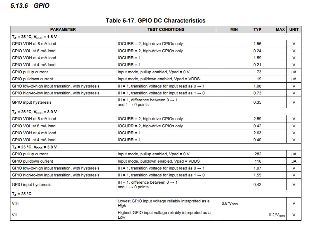
My MCU CC2642R VDDS is 3.3V. Therefore, 0.2 x 3.3V = 0.66V.
I knew it from another CC2642R post. It seems like VIH and VIL are the same as VOH and VOL respectively. I have a doubt on this too. VOH and VOL can't be found on datasheet at 3.3V supply voltage.
David, do you have the link to the E2E post you found about the VOH/ VOL levels? From how I read the datasheet I believe the answer you found is not correct.
First, VOH/ VOL will be very close to VDD/ gnd if you don't load the DIO. The data in the datasheet is measured with the max current the DIOs can deliver. If you look at VOL with 4 mA current the VOL is 0.21 V @ 1.8 V and 0.40 V @3.0 V which is less than 0.14*VDD.
I assume that you are not going to draw 4 mA from the DIO when you are using this as a control signal meaning that the VOL will be lower than 0.14*VDD.
I looked closer at the number and it looks like the spec (input to R&D) is 0.2*VDD/ 0.8*VDD as min/ max VOL/VOH when sourcing/ sinking 4 mA/ 8 mA. The number in the datasheet is typical.
The typical for VOH (4 mA source) is 0.88*VDD. If you are using a pull-up the current draw will be a fraction of this and VOL/ VOH will be much closer to the rails.
It's maybe easier to look at this at transistor level. Simplified, both the input and output are inverters.
For the output, lets say you want to output a logic '1', then the input to the inverter is a logic '0' to turn the PMOS fully on. If you don't have any load on the output of the PMOS, the drain-source voltage of the transistor will be low. But if you put a resistor from the output to ground the output voltage will be a resistor divider between the on resistance in the transistor and the resistor. So if you want to be close to the rail you have to have a large transistor and a small load.
For the input: We want a defined '1' or '0' from the output of the transistor. If VDD is 3 V and the input is 1 V (as an example) you have turned on both transistors in the inverter and the output will be somewhere in the middle. This is an undefined level (and increase the current consumption). For the input you normally don't sink any current, the levels defined are typically what you can apply to the input of the inverter and still have a logic level at the output.