This thread has been locked.

If you have a related question, please click the "Ask a related question" button in the top right corner. The newly created question will be automatically linked to this question.

UCC28064A: COMP relationship with maximum load

Part Number: UCC28064A
Other Parts Discussed in Thread: TIDA-010015, , UCC28064

Hello!

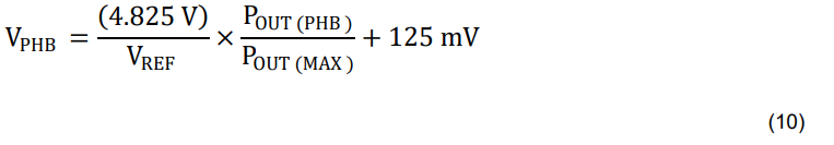
I am developing a 220-48V PSU based on TIDA-010015. I now have a problem of inconsistency between theory and practice regarding PHB and BRST pins. I saw on this forum somewhere, that this:

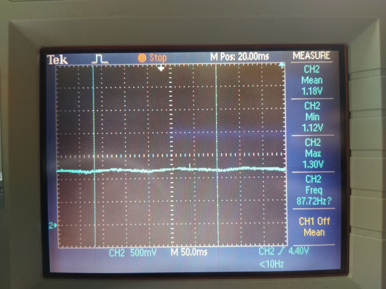
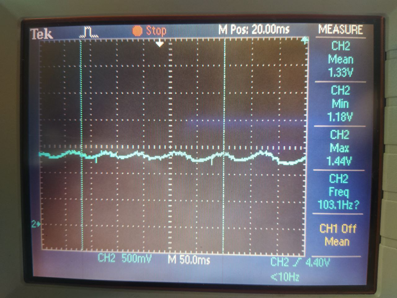
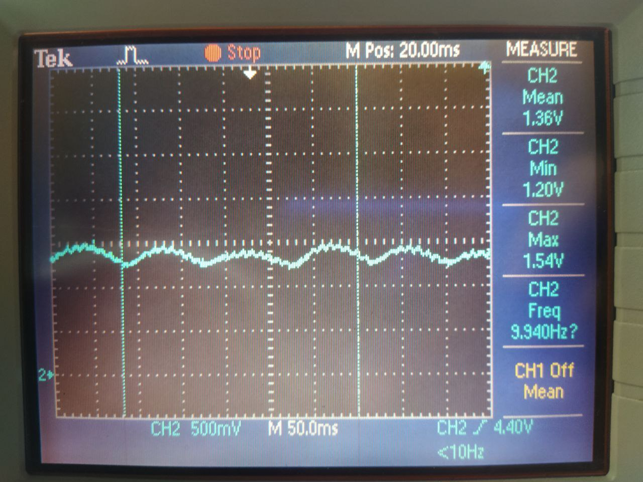
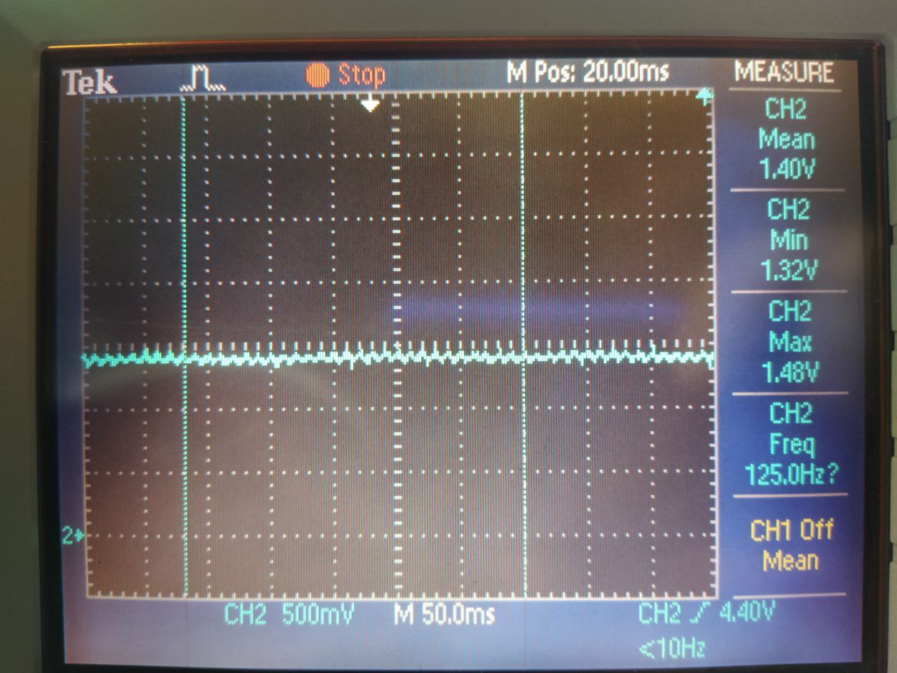
from page 22 of datasheet for UCC28064A is incorrect - there shouldn't be Vref. So with this taken into account, Burst mode and PHB thresholds are calculated so that they would be at approximately 60% of maximum power. I saw that at 50% load this design would come out of Burst mode and single-phase mode, which corresponds to calculations. So I changed R41 to 37.4 kOhms, R39 to 100 kOhms, R11 to 22.1 kOhms and R37 to 100 kOhms, so that BRST and PHD threshould would correspond to approximately 20% and 30% of maximum power (which by the way is set to 300 W by R7-R8, not 500W), and I still can't get the device out of Burst mode and single-phase mode at 50% of the load (meaning 150 W of load). 

I also looked at the functional block diagram (page 14 of datasheet for UCC28064A), and there COMP voltage depends only on VSENSE, not in any way (at least the way I see it) related to current and so almost independent of output power (though a bit related to the VSENSE change rate, which correspond to loading resistanse).

So, I guess, i'm asking about how output power is related to COMP voltage and, therefore, to coming out of Burst and single-phase modes?

Regards, Aleksey.

  • Hello,

    I reviewed the data sheet and the burst threshold trip point is set through the PHB divider.  So Vref should be part of the equation for setting burst mode threshold.

    The comp voltage controls the on time which is fixed for a given load and RMS input voltage. 

    1. Ipeak = (2*(Pout/efficiency)*2^0.5))/(Vinrms)

    2. Ton = (Lboost*Ipeak)/(VinAC*2^0.5)

    3. Ton = Vcomp*Kt, refer to page 8 of the data sheet Kt will be KTL, KTH, KTSL, KTSH depending on VINAC peak voltage.

    4.  Vcomp = Ton/kt = (Lboost*((Lboost*Ipeak)/(VinAC*2^0.5)))/(VinAC*2^0.5)

    Regards,


  • Hello again,

    Thank you for answer.

    Sorry for non-existing picture in the first message. I was referring to equation (10) on page 22 of datasheet. If I try to evaluate power level at which single-phase mode turns off in TIDA-010015, I'll get the power that exceeds maximum power of PSU by about 3 times. Could you, please, recheck that equation? Without Vref in denominator I get more reasonable 60% of threshold. Or could magical number of 4.825 be wrong here?

    Judging by your equations 1-3, relationship between load and Vcomp is quite straightforward, bigger the load - bigger Vcomp. Equation 4 gives me some very small numbers (something like 0.87*10^(-12)), maybe I am missing something? Anyway, judging by equations 1-3, at no load Vcomp will be almost zero, at full load Vcomp will be 2.5V for KTSH at 265V input voltage. But on my PCB I don't see such straightforward relationship, see pictures below.

    0 A (for 48V PSU) at ouput:

    1 A (for 48V PSU) at ouput:

    2 A (for 48V PSU) at ouput:

    3 A (for 48V PSU) at ouput:

    Is this normal waveform for this signal?

    I also get two-phase mode for PFC at about 4.5 A of output (48V), though I have a feeling that while having rid of one-phase mode, I haven't got rid of Burst Mode at this load. And sometimes, apparently, 2 channels of PFC are not interleaving, which I consider quite strange.

    CH1 - gate of channel B's MOSFET, CH2 - gate of channel A's MOSFET

    Regards,

    Aleksey.

  • Pictures don't seem to come through. I'll try again:

    0 A (for 48V PSU) at ouput:

    1 A (for 48V PSU) at ouput:

    2 A (for 48V PSU) at ouput:

    3 A (for 48V PSU) at ouput:

    CH1 - gate of channel B's MOSFET, CH2 - gate of channel A's MOSFET:

  • Hello,

    I believe the data sheet equation is correct.  You just may not be using the correct Kt?

    Typically these designs are designed for 85V RMS plus, I wonder if the KT values will not work down to 48V AC.

    Typically input under voltage is set at 60V RMS primary current run away.  Could setup the device to work from 85V to 220V to see if your power levels match what you expect.  The following link will get to the excel design tool which will help you reset up this device.

    https://www.ti.com/lit/zip/sluc645https://www.ti.com/lit/zip/sluc645

    Your gate drive waveform shows that you are in burst mode and coming in and out of single phase operation.

    You need to set these thresholds at two different levels so this misbehavior does not happen.

    Your comp voltage seems to be trying to correct for the 2X line frequency on the boost capacitor.  You might want to revisit the compensation on the comp pin.  The loop should cross over around 10 Hz. The excel design tool should help here as well.

    Regards,

  • Hello,

    48V is not input AC voltage, it's output DC. Input voltage is 220 V AC RMS.

    I was talking about this equation:

    Are you sure it is correct? I don't see how I can use here wrong Kt, because Kt is not used in this equation.

    And yes, my problem was connected to coming in and out of single phase operation. Turned out that if second phase turnes on, summarized power from two phases becomes too much for load to dissipate - voltage of PFC rises until it comes to either OVP threshold or just close to OVP which will cause switching to stop for a time (and also switch to single phase mode). Is that really a thing, or should UCC28064 be able to switch to two phase operation without such dramatic effect on output of PFC?

    Can you, please, elaborate on what you mean by "loop should cross over around 10 Hz". How is it done? I solved equations (56-59) on page 43 of datasheet for UCC28064 and got roughly the same values of components as those used in TIDA-010015. Is there any documentation that describes those equation down to basics? I am afraid I am a little ignorant on such matters.

    Regards,
    Aleksey.

  • Hello,

    I believe that equation is supposed to be derived from VREF/VPHB = POUT(MAX)/POUT(PHB).

    So I believe you are correct that VREF is not supposed to be in the denominator.  The 4.825V is supposed to represent VREF.

    I still think your issue is with PHB and burst mode being set at the same level.  Could you shift the PHB threshold up 200mV to see if the issue goes away.

    The data sheet gives a simplified loop compensation that should work to compensate the voltage loop.  However, the following application note describes how to compensate a CrM PFC and why the loop should cross over at 10 Hz.  This is so the voltage loop does not correct for the 2X line frequency ripple voltage on the PFC boost capacitor.

    Regards,

  • Hello,

    I reviewed this application note and that I get the best results with resistor of 15k and capacitors 2.2 uF and 180 pF for loop compensation.

    With those components installed instead of old ones, I still have some problems.

    I also learned that my problems considering second phase kicking at quite big load were, in fact, a consequence for setting up resistor on TSET pin, which is used for setting up maximum MOSFET on-time, too high (about 127 kOhms). 127 kOhms is a value estimated with respect to datasheet, whereas TIDA-010015 uses about 95 kOhms. At first I decided it was an error and installed 127 kOhms, but turns out that when 2-phase mode is set very high, only one phase (due to limitation by RSET pin) won't have enough power for PFC to have stable output voltage. Voltage will start to lower, which well eventually result in COMP voltage rising enough for second phase to turn on. Both phases will quickly make up for lack of voltage at the output of PFC, but accumulated error on COMP pin will cause overshoot, which will go to OVP or nearly OVP state, which, in turn, will cause second phase to turn off.

    At the time when previous pictures were taken resistors for BRST and PHB pins were as follows:
    Rd = 22.1 kOhms, Ru = 100 kOhms for BRST
    Rd = 37.4 kOhms, Ru = 100 kOhms for PHB

    So there was some margin between PHB and BRST, so that should not have been a problem. But as I described I had problem with PHB threshold set too high.

    Now I try to catch 2-phase mode threshold. For me to do this, I tried to measure COMP voltage to estimate needed voltage on PHB pin and I saw that at no-load COMP voltage would not equal zero or about zero volts. Instead, at no-load I get more that 1 volt at COMP pin. By increasing the load I get not very substantial increase in COMP voltage - certainly not enough to have reliable threshold.

    Following pictures are for resistors for BRST and PHB pins that are as follows:
    Rd = 17.4 kOhms, Ru = 63.4 kOhms for BRST
    Rd = 27.4 kOhms, Ru = 63.4 kOhms for PHB

    CH1 - COMP voltage with respect to GND, CH2 - 390 V at 0 A load for 48V output:

    CH1 - COMP voltage with respect to GND, CH2 - 390 V at 1 A load for 48V output:

    CH1 - COMP voltage with respect to GND, CH2 - 390 V at 2 A load for 48V output:

    CH1 - COMP voltage with respect to GND, CH2 - 390 V at 3 A load for 48V output:

    CH1 - COMP voltage with respect to GND, CH2 - 390 V at 4 A load for 48V output:

    CH1 - COMP voltage with respect to GND, CH2 - 390 V at 5 A load for 48V output:

    CH1 - COMP voltage with respect to GND, CH2 - 390 V at 6 A load for 48V output:

    So as you can see, I got about 300 mV for COMP voltage rise with about 300 W of load. Is this behaviour normal or something is wrong? From datasheet and various discussions i got the feeling that COMP voltage will swing from about 0 volts to no more that 5 volts for no-load and full load, is this right or actual behaviour is varying with different schematics/PCBs?

    If I then change PHB resistors to Rd = 19.1 kOhms, Ru = 63.4 kOhms (very close values to those of BRST resistors), I finally get 2-phase mode working at load of about 2.9 A (for 48V of output). Transition between 1-phase mode and 2-phase mode is not very clear - second phase sometimes kicks in, but most of the time doesn't work. With more load second phase blends in with first phase and switching is more clean and really interleaved, though it has some audible noise. Noise is an issue, but not right now.

    So I think that I finally got what I wanted and decide that, just to be sure, I would add some margin between PHB and BRST voltages. I can't make PHB voltage higher because otherwise I will miss out the 2-phase mode functrionality (due to too low COMP pin voltage change with load), so I will make BRST voltage lower. I decided to make Rd = 15 kOhms, Ru = 63.4 kOhms for BRST (which will give a voltage a little lower than that of COMP pin at no-load, but it is interesting to see result nonetheless). So I got interesting results.

    Following pictures are for resistors for BRST and PHB pins that are as follows:
    Rd = 15 kOhms, Ru = 63.4 kOhms for BRST
    Rd = 19.1 kOhms, Ru = 63.4 kOhms for PHB

    CH2 - COMP voltage with respect to GND at 0 A load for 48V output:

    CH2 - COMP voltage with respect to GND at 1 A load for 48V output:

    CH2 - COMP voltage with respect to GND at 2 A load for 48V output:

    CH2 - COMP voltage with respect to GND at 3 A load for 48V output:

    CH2 - COMP voltage with respect to GND at 4 A load for 48V output:

    CH2 - COMP voltage with respect to GND at 5 A load for 48V output:

    CH2 - COMP voltage with respect to GND at 6 A load for 48V output:

    So the mean COMP voltage at no-load and further got higher for about 400 mV. How is that possible? And also how is that possible that I am not able to get near 0V for COMP voltage at no-load at all? Can I do something to make COMP change more with load, so that I would be able to set PHB and BRST thresholds more reliably?

    Also thank you very much for your help, that PFC application note was very helpful.

    Regard,
    Aleksey.

  • Hello,

    Even at no load you have voltage dividers and other loads hanging off the boost capacitor.  This will require some kind of minimal switching to keep the design powered. It appears at no load to keep the output regulated the comp voltage does not have to go down to zero.  So your design seems to be O.K. 

    It seems like you have your design working.  If you need any more help please let us know.

    Regards,

  • Hello,

    Thank you for help. It appears, my problem was that feedback signals from either boost inductors were swapped. So only one phase worked fine even without feedback from inductor, but everything went to hell when second phase started working. That was quite stupid on my part, because this project was checked over several times for such errors.

    Regards,
    Aleksey.