This thread has been locked.

If you have a related question, please click the "Ask a related question" button in the top right corner. The newly created question will be automatically linked to this question.

TPS76901-HT: Reference voltage wirebond-configurable

Part Number: TPS76901-HT
Other Parts Discussed in Thread: TPS7A8300,

Hello,

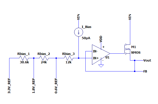
I was wondering if the bare die package allows for the reference voltage to be set by wirebond configurations.  I have seen voltage regulators for which the reference voltage is set by a bias current fed into a resistor chain.  And these parts would have bond pads connected at different points along this resistor chain that would allow the user to change the voltage reference bias resistor's resistance (thus voltage) by connecting to ground.  Is there access on the die to to do this, or does the reference bias topology even allow for this?  The figure below illustrates what I mean about configuring the reference via wirebonding.  For example, If I wanted to have a 3.3V output, I would tie the feedback and output together and connect the 3.3V_REF node to ground.  I could also connect the 1.8V_REF node to ground to easily get a 1.8V output.  I hope this makes sense.  

Regards,

Brandon

  • Hi Brandon,

    We have received your question and are currently looking into it. We will get back to you by 6/25/20.

    Regards,

    Nick

  • Hi Brandon, 

    This particular LDO is using voltage reference and the topology requires resistor divider between the output and the feedback to set the output voltage. We do have devices that use ANY-OUT pins to set output voltage but it still integrates the resistor divider. See example as TPS7A8300. 

    Our first LDO using the biasing current to set the reference is in development and it will have super low noise <1uVrms. May I understand why you would like to have this current bias topology to set the output voltage? How will it benefit your application? I am just trying to get more knowledge on your application so hopefully, I can help to propose something that works for you.

    Regards, 
    Jason Song

  • Jason,

    The schematic I posted is suppose to be a simplified representation of what's happening inside the LDO (not necessarily this LDO).  The I_bias would be the current source on chip used to set the reference voltage used by the internal error amplifier.  My thought is that if it is possible to change the LDO's internal reference voltage for the error amplifier, I could then directly feed the output back into the internal error amplifier non-inverting terminal.  This would allow me to reduce component cost and overall design footprint.  I am using the bare die component and will be wirebonding the die to a substrate.  Below is a block diagram showing another manufacturers part that has this capability (notice the resistor chain at the bottom and how the Vref can be changed by grounding one of the 10 reference pins).

  • Hi Brandon, 

    You just shared something that has marked as "confidential", you may need to delete the picture immediately from the public forum.

    Regards, 
    Jason

  • Jason,

    Thanks.  I deleted the picture.  This was actually from the datasheet available at X-REL's website.  So I don't know if this is really "confidential" or just a datasheet error.

    -Brandon

  • Hi Brandon, 

    Thanks for removing the picture. I got you what you mean for the current biased Vref, but I am confused about the application that mentioned as "directly feed the output back into the internal error amplifier non-inverting terminal". Yes, you could have the output connected back to the positive node of the error amp as shown in your first post, but then the gain would be negative. 

    The output voltage is already part of the control loop with either unity gain (FB=Vout) or a gain set by the resistor divider. So what are you trying to achieve?

    Regards, 
    Jason

  • Jason,

    The confusion is due to my typo.  I meant to say that the output voltage could be tied directly to the inverting terminal of the error amplifier.  The goal is to have unity gain, where the output is set directly by the error amplifier's reference voltage, with the hope that the reference voltage can be set to 3.3V, 1.8V, etc. by simply wirebonding a pad to ground.  I hope that makes sense.

    Regards,

    Brandon

  • Hi Brandon, 

    Okay, it makes sense now. Using this diagram as an example, instead of setting the NR pin voltage by the previous gained up bandgap voltage, you could use different resistors and biased current to set the reference voltage, and having a unity gain on the next stage error amp. Yes, we could definitely use different bond pads for different output voltages, as I said, our first current biasing based reference LDO is in development, and I can definitely check with the development team to see if they have a plan as you suggested to offer different output options. Is this what you need? 

    Regards, 
    Jason

  • Jason,

    I think we are on the same page now.  What I would like to know if this is possible with the TPS76901-HT.  In the datasheet, the wirebond diagram shows that a row of DNC pins exist at the bottom of the diagram.  And since these are close to the feedback pin, I thought these might be related to setting the reference voltage.  I included the photo from TI's datasheet and marked it to show what pads I am talking about.  Any information I can get about how these pads relate to the internal reference voltage (if they even relate at all) would be greatly appreciated.

  • Hi Brandon, 

    I only see HKJ, HKQ and DBV for TPS76901-HT, where did you get this footprint? What package is this?

    Regards, 

    Jason Song

  • Jason,

    This footprint is the known good die, and the pad layout is shown on page 3 of the the datasheet:

    https://www.ti.com/lit/ds/symlink/tps76901-ht.pdf?ts=1593212108134&ref_url=https%253A%252F%252Fwww.ti.com%252Fproduct%252FTPS76901-HT

    Regards,

    Brandon

  • Hi Brandon, 

    I don't think you could do this with this part, as the part was not designed to change the voltage using different pads. The design itself is also using voltage-based reference other than the current biased reference. 

    Regards, 
    Jason Song