This thread has been locked.

If you have a related question, please click the "Ask a related question" button in the top right corner. The newly created question will be automatically linked to this question.

UCC28056: Not regulating - Believe ZDC/CS voltage is too high

Part Number: UCC28056

I have modified a circuit to use the UCC28056. When I apply a 120VAC signal, the output does boost and gets to about 340V (set to 390V) but with almost no power. If I draw a constant 5W load, the output bounces around from 280V to 340V. 10W makes it drop to 100V, it is just all over the place.

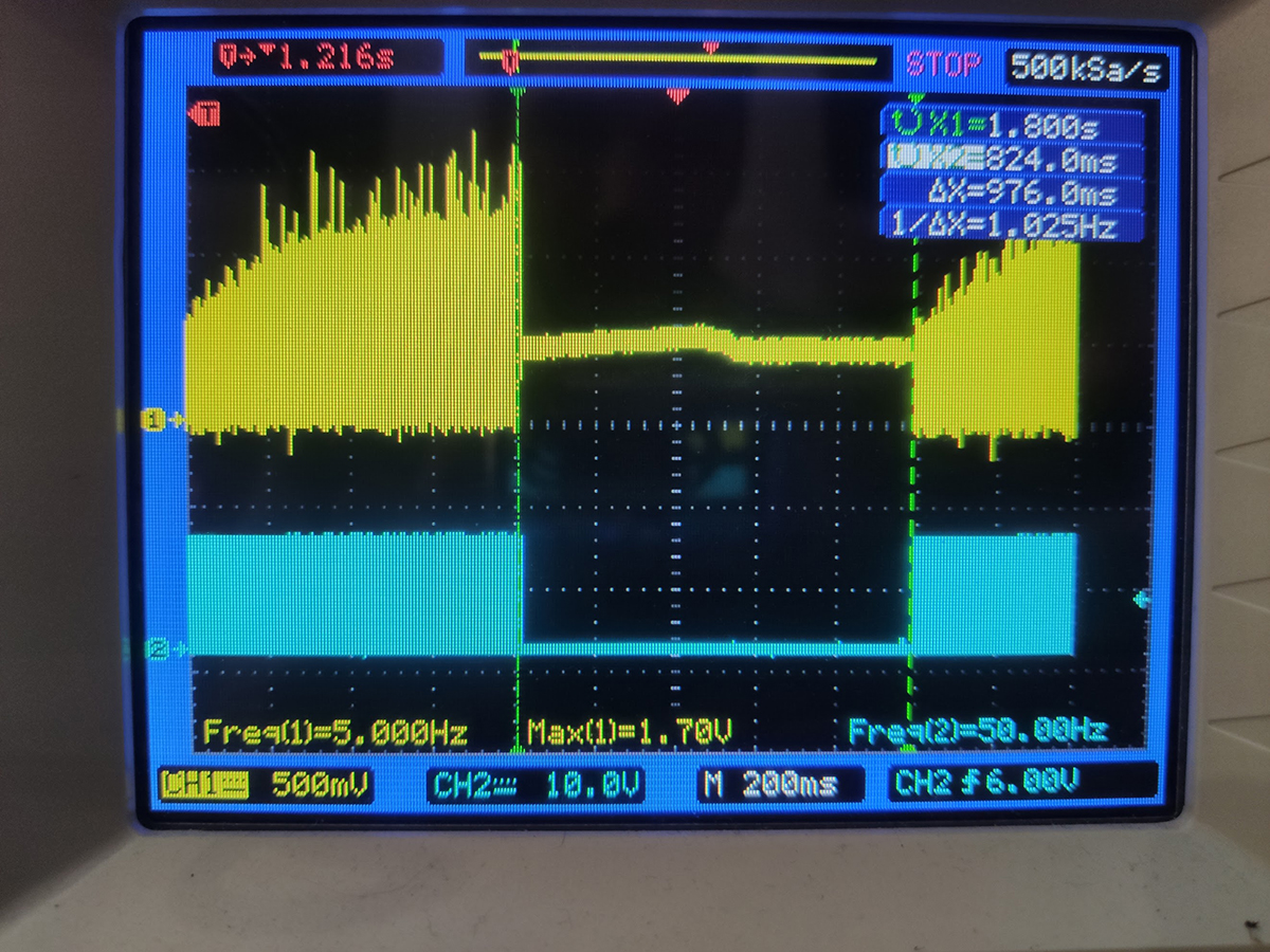
Looking at the ZDC waveform on the scope it appears to be too high. I am uisng essentially default values, trying to get the circuit operating before I tune it. 10Mohm with 10pF parallel from the FET drain to ZDC and then 26.1KOhm with 3.9nF in parallel from ZDC to FET Source / Current Sense resistor. It appears that a voltage over 500mV will cause the part to go into an OC #1 fault, and over 750mV will cause the part to go into an OC #2 fault. I believe I am getting OC #2 fault. I see 700mV to 800mV on the ZDC signal. It also follows a half-wave sine shape of 60Hz which makes it go up almost 600mV. Using the default circuit I did not expect to debug it and again without a real simulation environment like SPICE I am left probing the actual board to learn what is going on which makes this tedious.

What's going on, and is this the correct path to go down, trying to correct this ZDC waveform?

  • Hello Nick52556,

    Thank you for your interest in the UCC28056 PFC controller.

    Generally, when a circuit misbehaves very badly during actual operation even when the simulation works well, it is because of some mistakes on the prototype.
    These mistakes can be: incorrect component values, backwards polarized components, improper connections, and self-interfering noise from stray magnetic and electric fields.

    These errors are never modeled in the simulation, which is why every design must be debugged on a real prototype board, even if the paper design is perfect. 
    In this case, since the bad operation seems to become worse as the load is increased, I suggest to look for switching noise coupling from the main MOSFET into your voltage feedback pin VOSNS, or the ZCD/CS pin.   

    Regards,
    Ulrich

  • Yes but I don't have a simulation other than the webbench since TI doesn't provide a SPICE model as required. So I can't probe what the waveforms are supposed to look like ideally in simulation, and the datasheet is very limited with the waveform graphs so it is flying blind. The circuit behaves badly and has the proper components. But without knowing what the signals are supposed to look like, it is basically useless to try and debug.

  • Hello Nick52556,

    The following documents (found in the UCC28056 product folder on the TI website) have many different views of various waveforms. 

    https://www.ti.com/lit/pdf/slua920

    Unfortunately neither of them contain a capture of the MOSFET or boost inductor current during a switching cycle.
    The illustrations in the datasheet, Figures 19, 21, 24, and 27 are good representations of the expected current waveshapes.

    Regards,
    Ulrich