This thread has been locked.

If you have a related question, please click the "
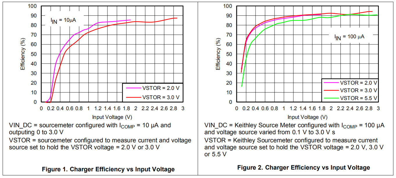
Ask a related question" button in the top right corner. The newly created question will be automatically linked to this question.

BQ25505: Can the charging efficiency diagram in the BQ25505 data sheet be simulated by software?

Part Number: BQ25505

The BQ25505 model is encrypted and cannot be simulated by Tina. Then how can the charging efficiency diagram of the charging management chip data manual be obtained? Can it be simulated by software (such as Cadence)?Besides building the test platform, can we use other software to simulate the charging efficiency diagram in the data manual?The following figure:

  • Hi,

    I am not aware of a discontinuous mode efficiency model for a boost converter. It is possible but time consuming to build a DCM boost converter in a spice simulator and then average the voltage and currents of transient simulations at different dc operating points.

    Regards,

    Jeff

  • Hi,Jeff

    The output of the charge management chip sets VBAT_OV to output a certain voltage according to the external resistance network. The resistance voltage divider network is controlled by the external microcontroller, and the adjustable VSTOR voltage is output for different application scenarios. Is this idea true?

    Regards

  • Hi,

    In theory, you should be able to inject a dc voltage through a resistor to the VBAT_OV pin and adjust the voltage set per the VBAT_OV resistors.  However, this is has not been tested.  Also, the u-controller's dc voltage through the injection resistor and bottom VBAT_OV resistor will waste power all the time.  The charger only looks at the voltages on VBAT_OV every 64ms, leaving them floating otherwise. 

    Regards,

    Jeff  

  • Hi,Jeff

    First of all, thank you very much for answering my questions. Meanwhile, I will have the following questions:

    1. The charger only looks at the voltages on VBAT_OV every 64ms that means the VRDIV node is monitored to samples and holds the VSTOR voltage.In addition to power consumption, does this situation affect my dynamic adjustment though the resistor to set the output to dynamic output?If it is possible in theory, can my output also can be dynamically changed every 64ms?

    2. According to data manual 7.4.3 shows One way to avoid cold start is to attach a partially charged storage element.If VBAT_SEC connection a depleted energy storage components such as super capacitor and energy collector provided is not enough, lead to chip cannot exit cold start, but in BQ25505 VBAT_PRI we have prepared a primary non-rechargeable batteries, we can through the primary battery to charge the  VSTOR  above 1.8 V firstly to make the circuit out of cold start, so that the booster work?I think the principle should be the same with attach a partially charged storage element, please talk about your opinion, thank you very much.

    Regards,

  • Hi,

    Regarding 1, the VRDIV node only samples the VSTOR node every 64ms.  It does not hold that voltage.  You can see the sampling in datasheet figure 20. If you keep the existing resistor divider and inject a dc voltage through a 3rd resistor to the existing resistor divider's midpoint, you should be able to dynamic adjust the voltage.  The concept and equations for resistor sizing are explained for different device at the link below.  You will burn power through the resistor.

    https://www.ti.com/lit/an/slyt106/slyt106.pdf

    Regarding 2, /VBAT_PRI_ON and /VBAT_SEC_ON are controlled by the VBAT_OK thresholds.  So, at a minimum, you would need the partially charged element to be above your VBAT_OK threshold in order for /VBAT_SEC_ON to be stay low after battery attach.  Keep in mind, you must attach the battery when VIN_DC, VSTOR and VBAT nodes are < 100mV from ground or the internal PFET will not turn on as explained in the middle of d/s page 17.

    Regards,

    Jeff