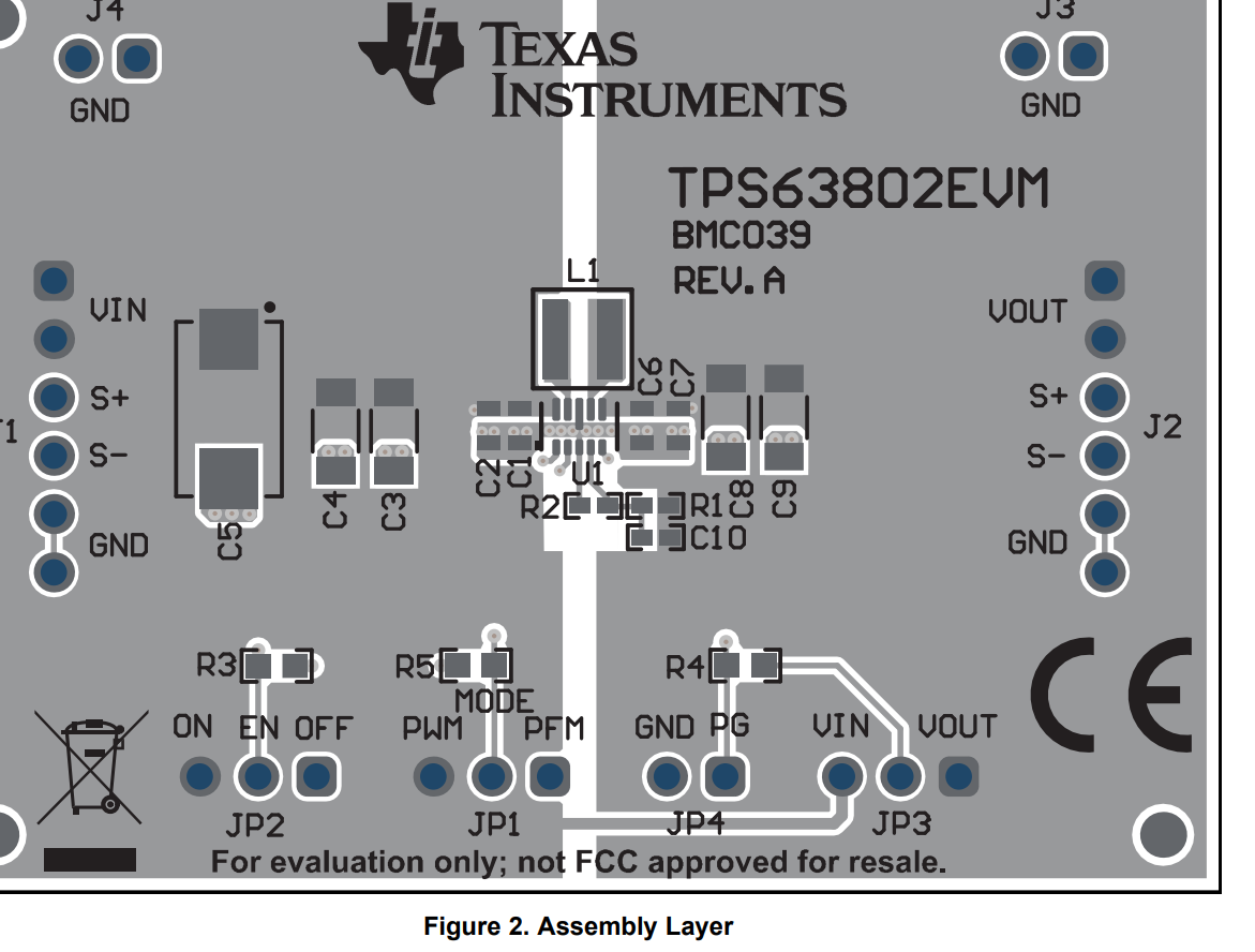
I do not understand this layout of TPS63802. two attributes emphasized in this layout are;
1) input and output bypass capacitors of the regulator is connected to the middle ground pad of the regulator but not connected to the ground plane on the same layer. Regulator and bypass capacitors are isolated from the top ground plane.
2) regulator ground plane on the top layer is cut into half!
I already implemented 1), but for 2), it doesn't make sense to me! Why do we need to split the top ground when all/most of the components are grounded on the inner layer?
If you can explain why 1) and 2) are done, it will enrich my knowledge. Thanks.


