This thread has been locked.

If you have a related question, please click the "Ask a related question" button in the top right corner. The newly created question will be automatically linked to this question.

ISO5452: ISO5452 design review

Part Number: ISO5452
Other Parts Discussed in Thread: ISO5451

Hi,

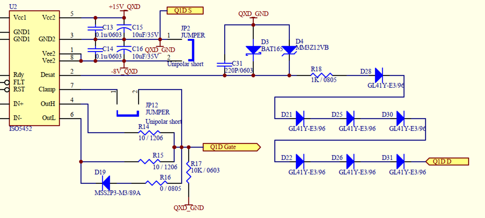
The attachment is the IGBT I used. I didn’t understand very well when designing the ISO5452 pin 2 Desat function, so please help:

1. D4 design considerations, how many volts do I need to take? Is 12V Zener ok for this? 

2. Is the number of D28/D21/D25/D30/D22/D26/D31 correct with IGBT? for used the IGBTRGTVX6TS65D

3. in my understanding, the number of the is VCE-FAULT(TH) = 9 V – n × VF, only need 1~2 diode, is that right?

The IGBT and D28~D31 SPEC as the attached PDF file

bym10-xxx-1767895.pdf

rgtvx6ts65d-e.pdf

Regards,

Rock

  • Rock,

    Thanks for your question. I very much appreciate you for providing all the relevant datasheet!

    Rock Shao said:
    1. D4 design considerations, how many volts do I need to take? Is 12V Zener ok for this? 

    12V zener is perfect.

    Rock Shao said:
    2. Is the number of D28/D21/D25/D30/D22/D26/D31 correct with IGBT? for used the IGBTRGTVX6TS65D

    Should not have as many as they had put , and you are correct that 1-2 would be best.

    The GL41Y-E3 diode  D28 and on have a forward voltage of 1.2 V, that means that a VCE voltage of just 0.6V will begin to trigger the DESAT, as 7*VF=8.4 + VCE <9V for no desat detection. Typically see the threshold as closer to ~7-8V, so one or two of the diode would be better otherwise they might see a lot of false tripping of DESAT. In fact, the DESAT detection threshold they have set is below the VCE(SAT) for their IGBT! Unless they have some explicit reason that they need the threshold so low,  I would say they need to reduce the number of those diode.

    Rock Shao said:
    3. in my understanding, the number of the is VCE-FAULT(TH) = 9 V – n × VF, only need 1~2 diode, is that right?

    Yes!

    Please let me know any further questions. If this answered your question, please let me know by pressing the green button.

    Best

    Dimitri

    1. D4 design considerations, how many volts do I need to take? Is 12V Zener ok for this?

  • Rock,

    Also, i had another note regarding this Diode D19 in the datasheet which has a 0-ohm resistor at the cathode. I am not sure why it is there but i see potential problme. On turn-off, the VGE of the IGBT is >> forward voltage of this diode, so no current will go through R15 until the voltage at the gate is below even the miller clamp threshold. So essentially the entire turn-off is dictated by the D19 diode, practically none of the turn-off current will go through R15.

    This will cause an uncontrolled turn-off where the VGE voltage will quickly drop with a large turn-off current, it may cause driver or system problems.

    A brief calculation is [VDD-VEE-VF(D19)]/ROL <- of gate driver, where ROL is the effective driver turnoff resistance from OUTL pin to VEE at 4Ohm, VF around 0.5V of D19, estimtate around 5.6A peak.

    This is technically exceeding the maximum sinking current of ISO5452, and I am not sure about the purpose of splitting the turn-off path with D19 in one path and 10ohm in the other path, because the 10ohm will have limited effect to limit the discharge current. . Possible cause of using this diode could be very large dV/dt of VCE of this IGBT, which can cause gate ringing at least and potential other problems in the system.

    Please check with the customer about the reason for adding D19 and that uncontrolled turn-off path since i believe it may be problematic.

    Best

    Dimitri

  • Hi Dimitri,

    You explained very clearly, thank you very much! Let me reorganize the current discussion

    1. 

    The GL41Y-E3 Vf = 1.2 V

    The RGTVX6TS65D VCE(SAT) = 1.9V

    For that number of those diodes means I need to check the IGBT VCE(SAT) right?

    and the following

    VCE-FAULT(TH) = 9 V – n × VF

    1.9V=9V-n*VF

    n=5.9

    Choose n = 1~2 diodes to avoid tripping of DESAT.

    2.

    In your explanation, the problem of D19 was mentioned. I saw D4 and R12 in the EVM circuit diagram(the same as the customer D19 and R16 circuit diagram) was DNI.

    Does this mean that the customer does not need to?

    If my customer really needs to use it, are there have any diode suggestions?

    But in my understanding, D19 and R16 is the discharger when IGBT turn-off. 

    The EVM circuit diagram

    Regards

    Rock

  • Hi Dimitri,

    And my customer wants to know about DESAT's working theory, did you have more about ISO5452 introduction? Or can describe the theory of this PIN?

    Thanks.

    Regards

    Rock

  • Rock,

    The basic theory is as follows: The IGBT should operate in saturation region. When it leaves saturation region, it could be due to a short circuit for example, VCE across the IGBT rises and current rises. Basically, if this happens it can fatally destroy the IGBT.


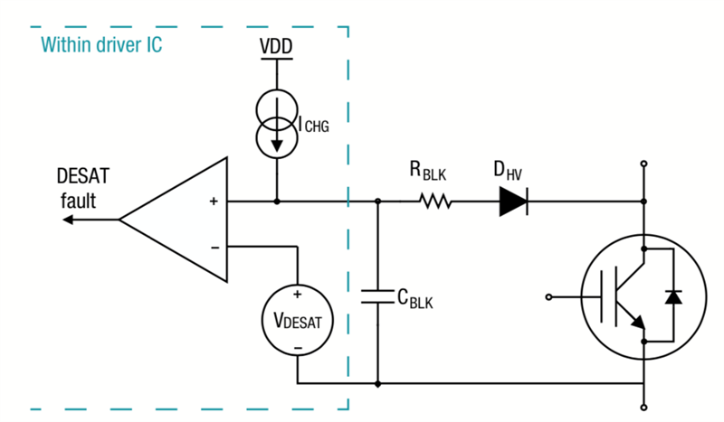
    DESAT is a method of detecting when the IGBT is "desaturating" or leaving the saturation regime. the driver monitors the voltage of DESAT pin. If it has been >9V for a certain time (called deglitch time, since we dont want false negatives), then the device will alert the primary side via the FLT pin going low, block any further inputs from primary side, and in the case of ISO5452, it will begin to discharge the gate via Soft turn off. This means current will be sinked from OUTL at ~140mA to slowly discharge the gate in a controlled manner which is order of magnitude less than the normal sinking/sourcing current. If it is discharged too quickly in this DESAT condition, the VCE can spike and lead to damage to the IGBT.

    The way the DESAT circuit works is like this.The ICHG sources current out of the pin. When IGBT is operating normally, VCE across it is low, so D_HV diode conducts the current and DESAT voltage is low. However, when the voltage starts to rise at VCE, this will be higher than voltage at desat pin, so DHV will stop conducting. The ICHG source will charge the Blanking cap. Once the threshold VDESAT>9V (longer than the deglitch time), the DESAT will be recognized.


    Regarding the parameters related to DESAT detection, they are located in page 10 of the datasheet, linked here.

    Timing diagram which helps to understand the waveform at each pin is located here

    Please see our ebook section on SiC/IGBT fundamentals, which has excellent explanations of DESAT purpose, design, and detection process. In fact i recommend the entire ebook it is an excellent resource that helps with a lot of questions.

    https://www.ti.com/lit/wp/slyy169/slyy169.pdf#page=29

    Also, a Comparison of Desat and Overcurrent detection methods

    If you have any more questions , please let me know. If this had answered your question, could you let me know by pressing the green button?

    Best,

    Dimitri

  • Rock,

    Rock Shao said:
    In your explanation, the problem of D19 was mentioned. I saw D4 and R12 in the EVM circuit diagram(the same as the customer D19 and R16 circuit diagram) was DNI.

    DNI means "Do not include" Or do not populate. There is absolutely no need for your customer to include placeholders or components like this for ISO5452 that i can think of . Please suggest them not to use them.

    The only reason that these footprints are used  in the EVM is for co-use the same EVM with ISO5451, which has single ended output unlike ISO5452 which has split-output. Bascially, the same PCB design are used for both, but the different components are populated.

    In ISO5451, OUT is the same pin (pin6) as OUTL, so it has those placeholders to allow for different turn-on/turn-off current by splitting the discharge path with the diode. From the perspective of ISO5452, they are not supposed to be populated and in fact they shoudl be ignored. As stated, i urge the customer not to use them at all.

    Rock Shao said:
    If my customer really needs to use it, are there have any diode suggestions?

    Your customer will not need to use it unless they were using ISO5451.  Please suggest them to remove it, its a bad idea to implement that.

    Best

    DImitri