This thread has been locked.

If you have a related question, please click the "Ask a related question" button in the top right corner. The newly created question will be automatically linked to this question.

UCC256302: Assumed ZVS detection timing

Part Number: UCC256302
Other Parts Discussed in Thread: UCC256402

Hi,

I saw the following thread.

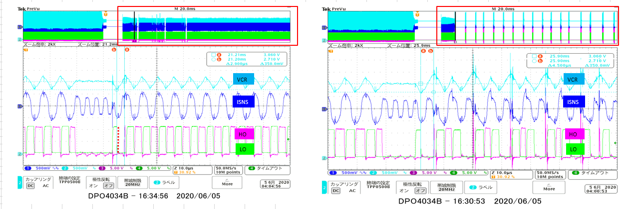
Mike-san commented that "I believe what your are observing is the converter detecting zero current switching ".

To confirm whether my understanding correct, I would like to know that the assumed ZVS detection timing.

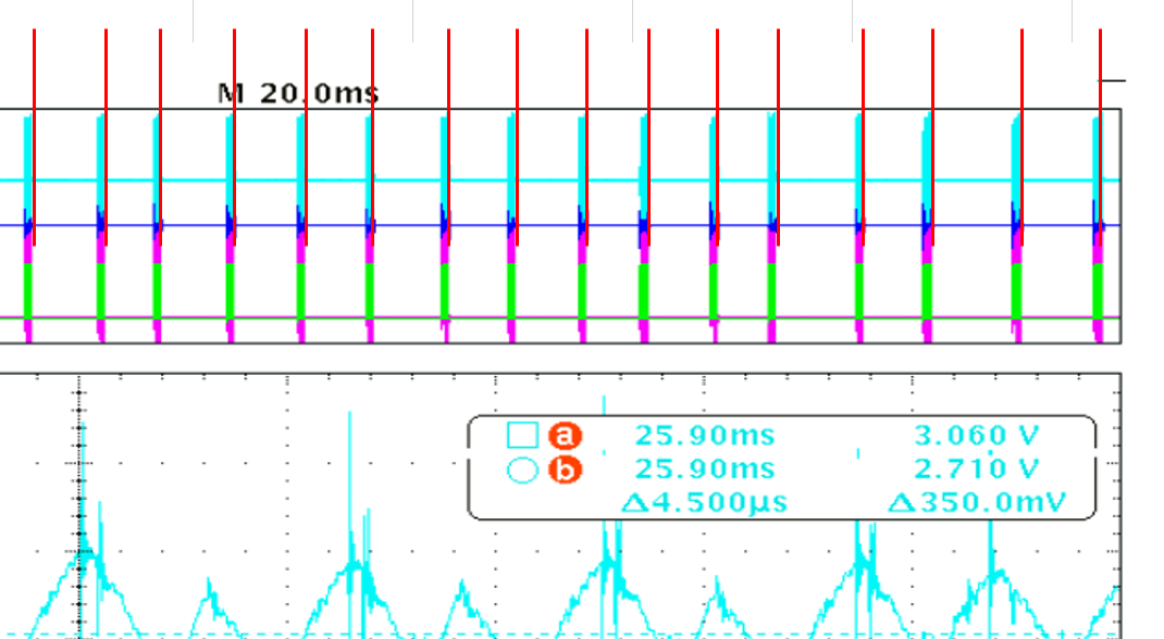
Is it assumed each red line timings on the following picture and the attached file?

TI_Inquiry 20200817.xlsx

Best Regards,

Kuramochi

  • Hi Tadahiko-san,

    The red lines in the image looks to refer to when the controller is at the end of a burst packet. In burst mode, the controller will stop switching when the feedback signal is smaller than the burst threshold programmed onto the LL/SS pin. As the output voltage droops due to no switching, the feedback network will start to increase the feedback signal. Once the feedback signal is larger than the burst threshold, the controller will start switching again. When the output voltage increases above the regulation set point, the feedback network will drive down the FB signal. Once the FB signal is smaller than the burst threshold, the controller will stop switching again. 

    The ZVS detection looks directly at the switch node. The HS pin needs to see at least 1V/ns to determine the switch node is in the process of "slewing". Once the switch node reaches either Vin or gnd, the dV/dt of the switch node drops to 0V. The controller sees this and uses this information to turn on the next gate.

    Best Regards,

    Ben Lough

  • Ben-san,

    Thank you for your quick advice.

    I understand what you wrote.

    And I would like to know why Mike-san believed that the converter is detecting zero current switching at the regarding thread.

    Do you know why?

    Best Regards,

    Kuramochi

  • Hi Tadahiko-san,

    I believe Mike O'loughlin is refering to the instances of missing slew rate detection in the burst mode waveforms. When slew rate detection is missed, the iSNS polarity change is used to turn on the next gate. I would also like to mention that we have a newer version of this device (UCC256402) which is capable of much detecting much lower slew rates than the UCC256302 (UCC256302 can detect down to 1V/ns while UCC256302 can detect down to 0.1V/ns). The UCC256402 would be better equipped to successfully detect the switch node slew rate at light load conditions such as this.

    Best Regards,

    Ben Lough

  • Hi Ben-san,

    I appreciate your kind and great support.

    I understand the behavior of observed waveforms.

    I would like to clear also regarding coming out of the burst.

    There are two waveforms as below.

    As you can see inside the red rectangle, the left side comes out of the burst soon but the right side does not come out of the burst.

    These are the same schematic and the load condition, but boards are different.different

    We would like to know why behaviors are different by boards.

    Should we observe LL/SS pin to look into the cause?

    Please let me know if there is another what we should do. 

    And, the right side waveform is high frequency of missing SR detection much than the left one.

    Do you think that it is related to not coming out of the burst?


    P.S. Unfortunately we can not change from UCC256302 to UCC256402 by scheduling.

    Best Regards,

    Kuramochi

  • Hi Tadahiko-san,

    It may be related to tolerances on the LL/SS resistors or transformer that is giving only marginally successful slew rate detection. I would suggest the following:

    1. most designs include a diode in the HO/LO gate drive paths to allow for independent turn on and turn off speed. If your design includes such a circuit, I would suggest trying to increase the turn off speed of the gate drive..

    2. Change MOSFETs to lower Coss. The lower Coss will allow for a faster switch node slew rate

    3. use a higher burst mode setting. A higher burst mode setting will have larger magnetizing current amplitude which will help with achieving the dV/dt criteria

    4. Reduce any snubber capacitance on the switch node if possible

    5. Reduce the magnetizing inductance of the transformer to increase the magnetizing current at light load.

    Best Regards,

    Ben Lough

  • Hi Ben-san,

    Thank you for your quick response.

    Are tolerances on the LL/SS resistors or transformer related to coming out of the burst or missing SR detection or both?

    And my understanding is that your five suggestions correspond to not coming out of the burst but missing SR detection.

    Is it correct?

    Best Regards,

    Kuramochi

  • Hi Tadahiko-san,

    it would be related to both SR detection and LL/SS setting tolerance. My suggestions are related to improving the slew rate detection reliability. I believe the reason you are seeing these longer periods of no switching is related to the missing slew rate detection. If the time between the burst packets is ~150us, then this indicates the switching is corresponding to the max dead-time timeout. So if this is the case, the periods of no switching is happening because the controller did not detect the slew rate and could not reliably detect the ISNS polarity change so the controller waited for the dead-time timeout (150us) before turning on the next gate.

    Best Regards,

    Ben Lough

  • Ben-san,

    Thank you for your assumption.

    it makes sense.

    Best Regards,

    Kuramochi