This thread has been locked.

If you have a related question, please click the "Ask a related question" button in the top right corner. The newly created question will be automatically linked to this question.

LM3481: DR Pin8 showing two levels

Part Number: LM3481

Hello,

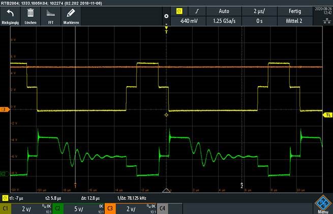
we have a flyback design using LM3481. Vin is 5.3V. We measure 5V at the VCC pin buffered with 1uF. As we are blow 6V the internal BIAS circuit should be disabled and the Vin voltage forwarded to the VCC pin. The VCC pin voltage should driving the DR pin8 and Vgate. In series to the gate we are using a 1Ohm resistor. However, VCC with 5V seems to be different from the DR Voltage which rather equals Vin.

Current sense resistor is 220mOhm setting around 700mA peak limit which we do not hit. From time to time we do see a switching waveform of the DR pin and the VDS of the FET which seems to be like tow levels. The DR Pin does not switch from 0V to VCC but has a step in between. Please see the attached scope plot.

What is the explanation for this?

We can repeat this with several boards.

Orange: VCC

Yello: VGate

Green : VDS

many thanks

Lutz

  • Hi Lutz,

    Thanks for reaching out with your question and for using the LM3481.

    Can you please post the schematic? I have not seen a issue like this on the gate drive before. If you cannot share the schematic publicly  please send it to me over email. Just to confirm, this only happens when the input voltage is close to 6V, correct?

    Please let me know if you have any questions.

    Thanks,

    Garrett

  • Hi Garrett,

    thanks for you help. I will send you some material offline. But the good news is we found the problem. The trigger perfromance of a Rohde & Schwarz scope was causing it. Using the old Lecroy everyhing works as expected.

    kind regards

    Lutz