This thread has been locked.

If you have a related question, please click the "Ask a related question" button in the top right corner. The newly created question will be automatically linked to this question.

TPS548B22: Related Thread: Reopen of Issue with TPS548B22

Part Number: TPS548B22

Hi Gerold,

This is a related Question : https://e2e.ti.com/support/power-management/f/196/t/848080

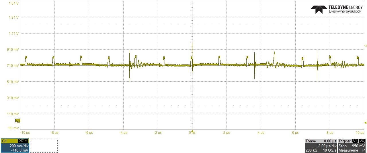
I have completed the design using TPS548B22 for Generation of 0.72V

But below is the observed output after fabrication and assembly

https://e2e.ti.com/cfs-file/__key/communityserver-discussions-components-files/196/7e055fe4.png

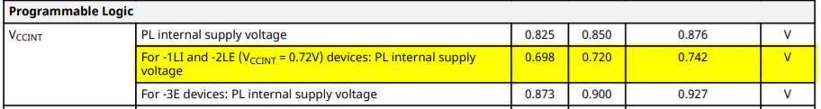
The recommendation from the FPGA OEM is as below

https://e2e.ti.com/cfs-file/__key/communityserver-discussions-components-files/196/3377.image001.jpg

Why is the over shoot in voltage ?

Schematic Implemented :


I have used a external independent regulator to enable it, not any PMIC.

Scope shots at output node and switching node are as below


  • Hi Shyam,

    This very large measured output ripple could be due to the measurement setup. It looks like the switching node is coupling to the measurement.

    Please take a look at the link below. Typically we use the pig-tail method and 20 MHz bandwidth limited. I also recommend measuring across the output cap closest to the load to minimize radiated noise being picked up by the probe.

    https://e2e.ti.com/blogs_/b/powerhouse/archive/2016/07/27/how-you-measure-your-ripple-can-make-you-or-break-you

    Anthony

  • I Measured across one of the output cap using pigtail technique, you were true, output is as below.

    but what i could not understand is 

    i was expecting it to be a a pulse and then discharging curve with in limits, but rather how come its perfectly a pulsating with a PRF, is this the expected ouput ? or still there is noise coupling somewhere ?

    but how should i check what is reaching the FPGA core, has it got coupled with noise ? i only have a test point of core voltage.

  • Hi Shyam,

    Glad to see that the different measurement improved the result.

    This type of output ripple waveform is dominated by parasitic ESL of the output capacitors and PCB. There is an inductive divider from the switching node to the output. With relatively output inductance value, the inductance between the output and ground becomes more significant. For example with only 300 pH effective inductance in series with the output caps, you would expect to see 12V*0.3nH/(200nH + 0.3 nH) = 18 mV. With lower output inductance it doesn't take much parasitic inductance to cause more output ripple.

    To reduce the ripple, try to reduce the parasitic inductance in the PCB layout and/or use ceramic output capacitors with smaller package sizes. Smaller package sized ceramic capacitors should have less parasitic inductance.

    Generally I would expect the ripple at the FPGA core to be slightly lower than measured near the output of the converter. Parasitic impedance of the PCB traces can provide a small amount of additional filtering. I suggest measuring as close as is practical to the FPGA.

  • One more issue i am currently facing is how to use the pgood for enabling other device like PMIC

    is it mandatory to tie it to BP ?

    rather can i pullup it with  a 3v3 rail of PMIC ?

    if i pull up it to BP, the voltage read is 5v, which cannot be tolerated by the enable pins of pmic

    kindly suggest a way out

  • Hi Shyam,

    For this device it is ok to pull PGOOD to another rail on the board. As noted in the datasheet, the PGOOD pin can pull down as soon as VDD is at least 1.2 V. So, the PGOOD signal will be valid at this point.

    Anthony