This thread has been locked.

If you have a related question, please click the "Ask a related question" button in the top right corner. The newly created question will be automatically linked to this question.

ISO5852S: Can it be used as a high-side gate driver

Part Number: ISO5852S

Hi,

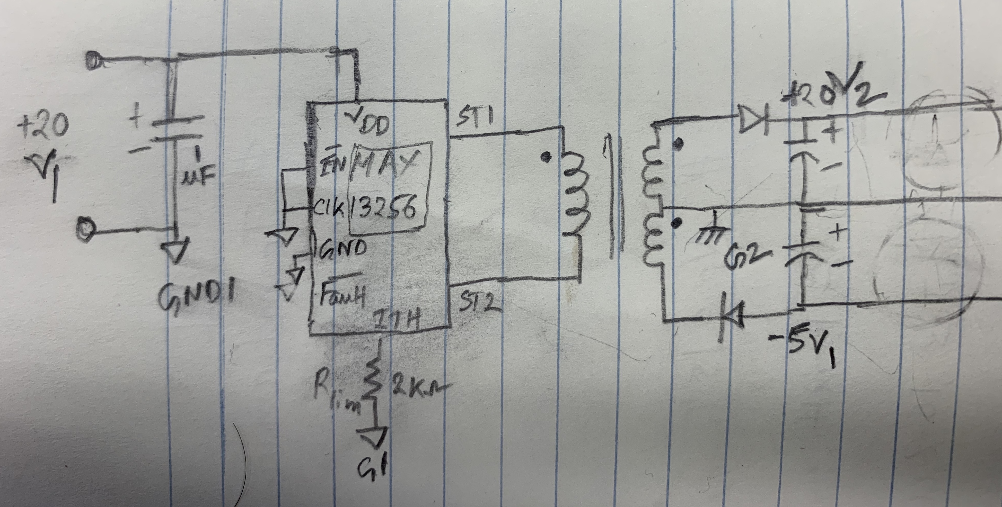
I am planning to use ISO5852S as a high-side gate driver using a bipolar supply. One of the main reasons behing choosing this IC is a seperate Vee pin. I plan to provide  +20V and -5V from the secondary winding of a transformer and the common ground point of those two rails will be connected to the GND2 pin of the IC (A basic schematic of the voltage rails of the transformer and the common ground is posted below for reference). I am planning to use this gate driver to drive a series stack of MOSFETs at a supply voltage upto 5 kV in a high-side configuration. My questions are as follows.

1. Is my understanding of the bias/power supply connection to the gate driver IC is correct?

2. Can the gate driver be used in a high-side application?

Thanks in advance.


  • Here is the schematic that I forgot to attach in my original post.

  • Hi Wesekul,

    Welcome to E2E!

    Your understanding of the bias power supply connection is correct. The positive supply would be the connection to VCC2 and negative supply to VEE with their common reference being GND2.

    The ISO5852S shouldn't have a problem in a high side application.

    Feel free to create a new post or continue off of this posts if you have any more specific questions about your design.

    Best regards,

    Andy Robles

  • I have another question regarding high-side connection. The recommended 220 pF capacitor connected to the CLAMP pin of the IC is connected to GND2 in the datasheet (for low-side configuration). For high-side configuration, my understanding is that the capacitor should not be connected to the ground. Am I correct?

    Thanks in advance.

  • For high side configuration, the capacitor should be connected to the GND2 of the high side device (Source of the high side MOSFET).

    By the way, ISO5852S has working voltage limitation as 1500Vrms, 2121 Vdc according to VDE standard (datasheet page 7), so if you have 5kV across the driver primary and secondary, that is not within the datasheet spec.

    Regards,

    Gangyao

  • Thank you for the feedback. In my previous post, I have mistakenly mentioned CLAMP pin instead of DESAT pin that might have caused confusion. From Fig. 50 (datasheet,page 26), I see that the DESAT pin is connected to the Drain of a MOSFET and Source of the MOSFET is connected to a GND and a 220 pF capacitor is connected between the GND and the DESAT pin. It is not shown (for the bipolar supply, Fig. 50) whether this GND symbol (arrow) is referring to GND 2. Can you please confirm whether this GND symbol refers to GND2?

    I plan to use an isolation transformer for the bias supplies (Vcc1, Vcc2, Vee2) of the gate driver and optical fiber for the isolation of the PWM signal. In this scenario can I use this gate driver for 5kV operation or can you suggest an alternative (preferably with a dedicated Vee pin)?

  • Hi Wasekul,

    You are correct. The GND symbol you are referring to in FIgure 50 is referring to GND2.

    For your application conditions I will review them with the team and get back to you with a response and/or possible alternative solution by tomorrow 9/15.

    Best regards,

    Andy Robles

  • Hi Wasekul,

    The voltage limitation of the ISO5852S refers to the max voltage differential allowed between GND1 and GND2at all times. If the grounds in your system are designed in order to limit the voltage differential with some tolerance to the spec(1500Vrms, 2121 Vdc) then the driver should not have any problems in your application.

    Let me know if there's any questions. Sharing a schematic could also help me understand your system better to see if there's any concerns.

    Best regards,

    Andy Robles

  • Hi, 

    Thanks for the feedback. I have one more question regarding the connection to the CLAMP and RDY pin. If I don't intend to use these two pins, should I leave those two pins open or connect them to GND2 and GND1 respectively? 

    Thanks.

    Regards

    Wasek

  • Hi Wasek,

    If not used you can leave CLAMP pin open.

    For best practice RDY should be pulled up to VCC with a 10K for example, but leaving it open would also be okay.

    Best regards,

    Andy Robles

  • Hi,

    Thanks for the information. What would be the best configuration for the RST pin if I don't plan to use it? Should it be pulled up to Vcc as well with a 10k resistor?

    Thanks.

    Regards

    Wasek

  • Hi Wasek,

    The RST pin is not an output pin. RST is an input to the ISO5852S and should be pulled high in order for the output of the gate driver to operate. If no strategic reset configuration will be done then pulling this pin up to VCC through a 10K resistor would be fine.

    Best regards,

    Andy Robles