This thread has been locked.

If you have a related question, please click the "Ask a related question" button in the top right corner. The newly created question will be automatically linked to this question.

TPS65130: Schematic configuration inquiry

Part Number: TPS65130
Other Parts Discussed in Thread: CC2640R2F, OPA2991, TPS62840, , TPS65131

Hello. I wish to ask some questions preparing my TPS65130RGER prototype;

this is a project using a 3.7V Lipo battery powered CC2640R2F Bluetooth project.

This 3.7V battery will be connected to TPS62840 and TPS65130RGER where the boost converter TPS65130RGER will power OPA2991 Op Amp by creating ± 15V.

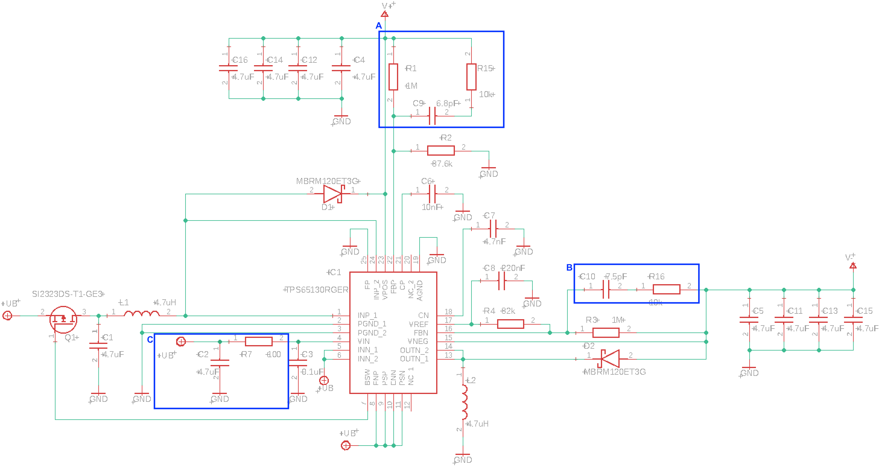
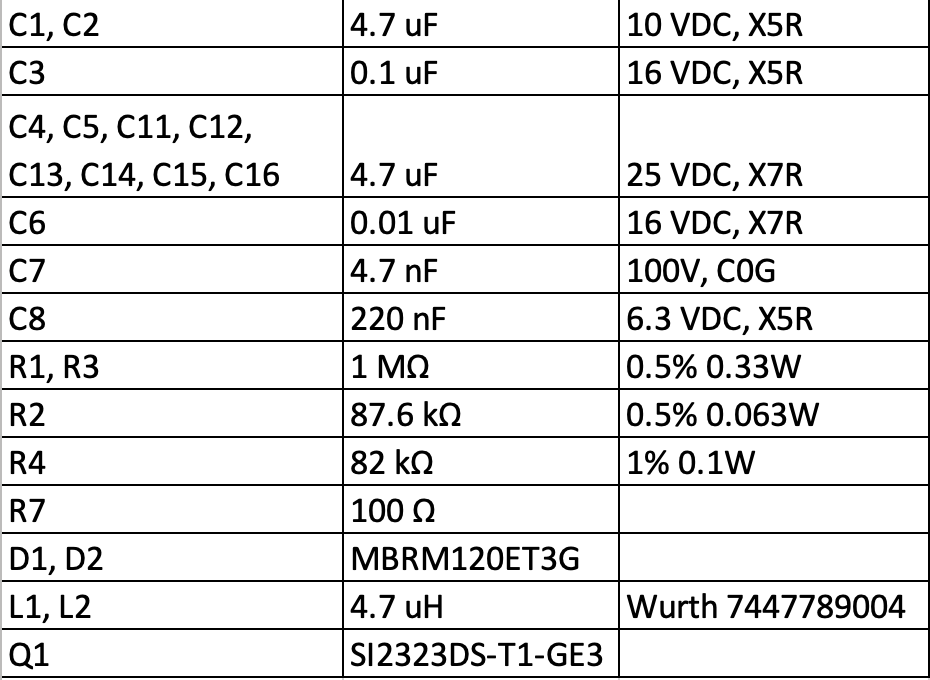
Here's my first draft of the schematic of the TPS65130 with the BOM;

My questions are

Q0. the WEBENCH Power Designer doesn't support TPS65130, right? I hope the WEBENCH support this device in the future.

Q1. when comparing the design from the TPA65130EVM-063

VS

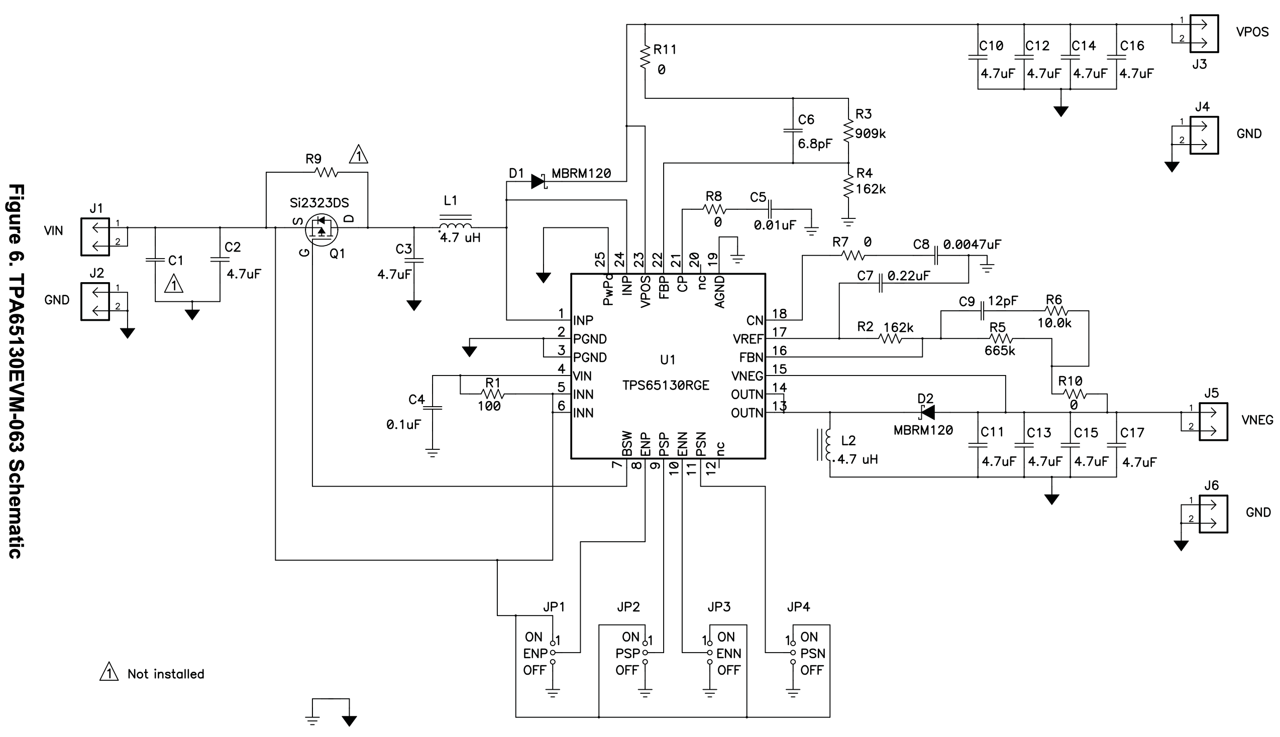
From the TPA65130EVM-063, the R5 || (R6 + C9) connection is different from the datasheet's R3 || C10.

Right now, I used the datasheet's calculation method

C9 = 6.8us / R1 = 6.8pF

C10 = 7.5us / R3 = 7.5pF

Currently, I copied the datasheet's design; which one should I follow and how was C9 from TPA65130EVM-063 was calculated?

Q2. About the four control pins (ENP PSP ENN PSN), can I connect all four pins to a single 3.3V/0V GPIO pin from the CC2640R2F MCU?

I only want to toggle a single GPIO to set the voltage to HIGH/LOW for these control pins.

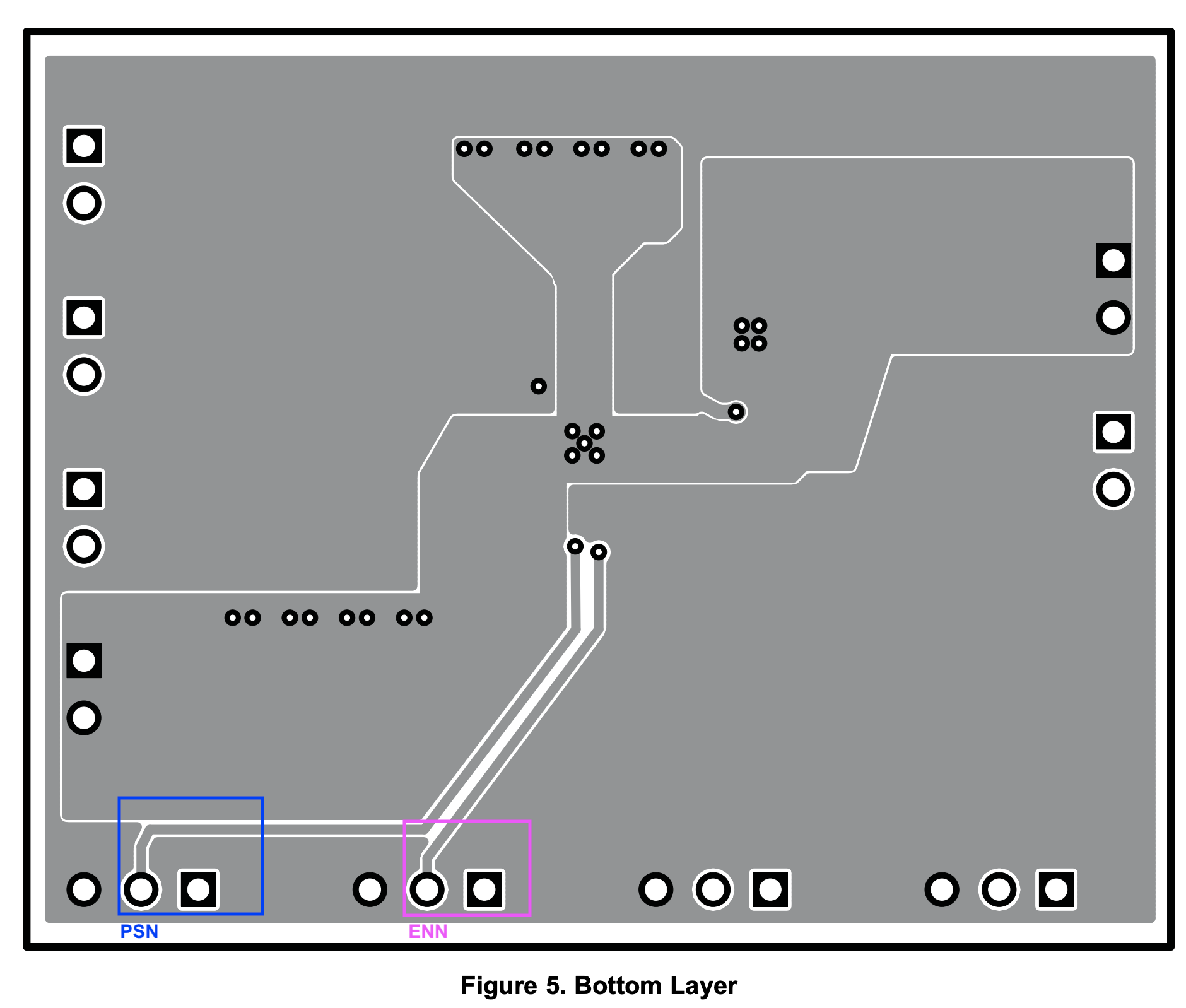
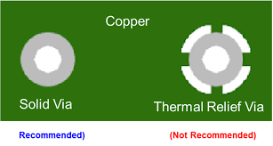
Q3. Another discrepancy; TPA65130EVM-063 has 5 thermal relief vias

whereas the datasheet example showed 9 vias.

I'm creating a 2-Layer PCB (FR-4, 1.6mm thickness) for my prototype.

What via size (Diameter / Hole in mm) and number of thermal reliefs are recommended to power the OPA2991 Op Amp when using a 3.7V LiPo battery?

I use EAGLE 9 and I was using this link to generate these vias.

Q4. Setting the voltages when V_ref = 1.213V,

R1 = R3 = 1 MΩ, R2 = 87.6 kΩ, R4 = 82 kΩ

R1 = R2 * (V_POS / V_ref - 1),     V_POS = V_ref * (1 + R1 / R2) = 15.060 V

R3 = -R4 * V_NEG / V_ref,           V_NEG = -V_ref * R3 / R4 = 14.793 V

The datasheet says

"The maximum recommended output voltage at the boost converter is 15 V. To achieve appropriate accuracy,
the current through the feedback divider should be about 100 times greater than the current into the FBP pin.

The recommended value for R2 should be lower than 200 kΩ.

The recommended value for R4 should be lower than 200 kΩ."

I want to achieve ± 15V. Do I need to change the resistors due to reasons like my current V_POS > 15?

Since '6.1 Absolute Maximum Ratings' says 'VPOS max 17V', I wish to check this part.

If there are additional changes needed in my schematic, please let me know. Thanks for your help.

  • Hello,

    We will review your post and get back to you with our feedback in the next couple of days.

    Kind Regards,

    Liaqat

  • Hello David,

    I reviewed your schematics and questions. Schematics looks good but I did notice that TPS65131 device Vin is not connected to any voltage and C2 is your schematics should be connected to +UB+ input supply.

    Now to answer your questions:

    A0: You are correct that web bench model for this device is currently not available.

    A1: C9 in the TPS65630EVM-063 was calculated with the same equation as what is in the datasheet and that you used for your design i.e. C10 = 7.5us / R3. Calculated value for EVM schematics comes out to be ~11.2pF so a 12pF capacitor was used. I do recommend to add a 10K resistor in series with C10 in your schematics similar to how it is in the TPS65130EVM-063 schematics. I also recommend to add a similar 10K reistor in series with C9 to V++ net. We added  these two resistors in the design to reduce noise coupling into the FBP/FBN pins through the feed forward capacitors C9 and C10 that was happening in some of the noisier customer designs.

    A2: All four control pins (PSP,PSN.ENP,ENN) can be connected to one GPIO.

    A3: Either five or nine thermal vias should be sufficient to remove heat from exposed thermal pad of the device to bottom side GND plane. Please provide as much bottom side GND copper as possible on your board for heat spread.

    A4 you can use any values of R2, R4 below 200K as recommended in the datasheet. You can adjust the divider ratio to achieve the proper output voltage desired in your application.

    I hope that this answers all of your questions.

    Kind Regards,

    Liaqat

  • Liaqat Khan said:
    Vin is not connected to any voltage and C2 is your schematics should be connected to +UB+ input supply.

    Thanks for your reply.

    Liaqat Khan said:
    A3: Either five or nine thermal vias should be sufficient to remove heat from exposed thermal pad of the device to bottom side GND plane. Please provide as much bottom side GND copper as possible on your board for heat spread.

    What via size (Diameter / Hole in mm) and number of thermal reliefs are recommended?

    Liaqat Khan said:
    A4 you can use any values of R2, R4 below 200K as recommended in the datasheet. You can adjust the divider ratio to achieve the proper output voltage desired in your application.

    Is R1 = R2 * (V_POS / V_ref - 1),     V_POS = V_ref * (1 + R1 / R2) = 15.060 V

    acceptable? I'm worried because this configuration exceeded 15V.

  • Hello David,

    5 vias of 0.2mm diameter should be enough. I suggest not to have any thermal relief connection around vias and instead connect the via pads solidly to the surrounding copper for better heat spread.

    V_POS setting of 15.06V should be okay.

    Kind Regards,

    Liaqat

  • Thanks, Liaqat.

    Liaqat Khan said:
    V_POS setting of 15.06V should be okay.

    Then how about

    V_ref = 1.213V, R1 = R3 = 1 MΩ, R2 = 87.6 kΩ, R4 = 80.6 kΩ (1/10 W)

    R3 = -R4 * V_NEG / V_ref,           V_NEG = -V_ref * R3 / R4 = -15.0496 V

    Is V_NEG = -15.0496 V acceptable?

    Back to your schematic feedbacks, where you've mentioned "Vin is not connected to any voltage and C2 is your schematics should be connected to +UB+ input supply." and others,

    I edited

    A. R15 - Added 10K resistor in series with C9 to V+ net to reduce noise coupling into the FBP pins through the feed forward capacitor

    B. R16 - Added 10K resistor in series with C10 to V- net to reduce noise coupling into the FBN pins through the feed forward capacitor

    C. Connected UB+ (3.7V battery voltage) to C2

    Am I following your recommendation correctly?

    Liaqat Khan said:
    I suggest not to have any thermal relief connection around vias

    Can you elaborate this part? I was thinking about imitating the design from TPA65130EVM-063.

     Like this design, do you mean signal traces like PSN, ENN, etc shouldn't pass the GND copper plane in order to provide as much bottom side GND copper as possible?

    I'm thinking of using FR-4, 2-layered 1.6mm thick PCB.

    One last question; when making a large GND copper possible, is there a minimum size, like 10mm x 10mm GND copper, in order to use TPS65130 providing 15V & -15V outputs?

  • Hello David,

    Your edits to the schematics look good and 15.06V and -15.04 for output voltages should be ok.

    Regarding the thermal relief for vias in the exposed center pad of TPS65131, I recommended no thermal relief, similar to how it is on the EVM board, because it will allow for better heat spread from exposed bottom pad of TPS65131 to surrounding copper.

    There is no minimum size recommendation for the GND copper but, obviously bigger is better for heat spread reasons.

    Kind Regards,

    Liaqat

  • Hello, Liaqat.

    Liaqat Khan said:
    I recommended no thermal relief, similar to how it is on the EVM board,

    Now I remember;

    You want this solid via, not a thermal relief via like this picture, right?

    I use EAGLE so I'll use this "no thermals option" to do this.

    Liaqat Khan said:
    Your edits to the schematics look good

    Just to double check, do you mean the 10K resistor in series with C9 or C10 is also good too?

    After this one, I'll close this ticket.

  • Hello David,

    Yes, the solid via as shown on your picture is good for better spreading heat.

    And yes, 10K resistors in series with C9 and C10 are also good.

    Kind Regards,

    Liaqat