This thread has been locked.

If you have a related question, please click the "Ask a related question" button in the top right corner. The newly created question will be automatically linked to this question.

TPS61023: TPS61023DRLR

Part Number: TPS61023

Hello TI Team, 
Myself Meghanath,

I'm using a TPS61023DRLR a Boost Converter IC in my design for the o/p voltage of 3.3V with a current of 50mA having input voltage of 3V from a coin cell battery.

I'm facing a following issues:

1) As soon we power up the HW, the o/p voltage dipping to 2.6V, FB voltage is dipping to 0.45V and SW- GND are shorted.
2) Then we built a Boost circuit in breakout board for the above mentioned values and tested,
     I) When we test without Load, the o/p voltage is 3.3V. FB voltage also coming fine (0.6V) which is typical.
     II) But when we connect a load of 330 ohm(10mA) , the o/p voltage is dipping to 2.6V. FB voltage also dipping to 0.45V.
     III) Same Scenario is observed with the different loads - 150 ohm (22mA), 100 ohm (33mA).

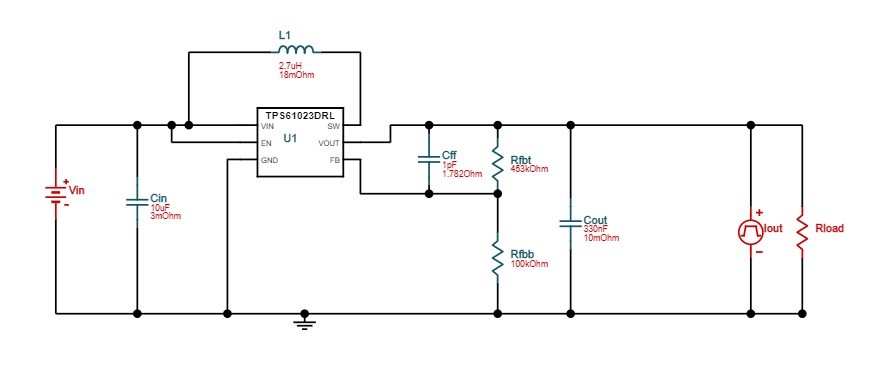
Below attached image is the designed circuit.

Output capacitors changed to two "22uF".


Please suggest a solution for the above issue.

Thank you.

  • Hi Meghanath,

    I noticed that the inductor L1 is marked with 1uH/100mA. Does it mean the inductor saturation current is 100mA? 100mA is too low for this application. Inductor could be saturated when load is applied. Please check it.

    Please also share the layout. Thanks.

  • Hi,
    Zack Liu

    In the image we have sent, yes the value is 100mA(because our design is for 50mA). But in the breakout Board, we have kept the inductor as 2.2uH(500mA).

    Also will that TPS61023 IC will work for low loads (10-100mA)?

    Thanks.

  • Hi Meghanath,

    100mA Isat value is too low for TPS61023. In your design, 50mA is the output current. For a boost converter, inductor current is a triangle waveform and the inductor current ripple would be several hundreds of milliamperes. The inductor current average current equals input current. In my experience, you'd better select a Isat=1A inductor for this application. 

    TPS61023 works for load current of 10-100mA. 

  • Hello Zack,

    I tried by putting inductor 3.3uH with Isat=5.9A, even though the result is same (dip to 2.6V when load is connected, without load output is as expected 3.3V).

    Also i tried the suggested ckt by WeBench, following is the ckt

    Changes in above ckt,

    1) O/p cap replaced by two 22uF
    2) Inductor replaced by 3.3uH as mentioned above.
    3) FB resistors, Rfbt=680K and Rfbb=150K

    Thanks

  • HI Meghanath,

    Thank you for the update.

    Could you quickly share the layout? Layout might be one reason to cause poor Vout regulation.

  • Zack,

    we are Testing it in a Breakout Board.

    Thanks

  • Hi Meghanath,

    It's not suggested to test power converter on breakout board because the trace parasitic inductance and resistance will affect the normal regulation. You could buy one EVM on ti.com to test.

  • Hi Zack,

    we tried by putting high current rated inductor in the Design Board (PCB) itself, even though the result is same.
    we have cross checked the design several times, no problem with the design.

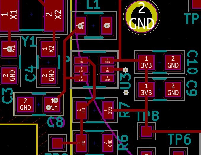
    the below attachment is layout design

    C8 = input cap, L1 = Inductor, C9 & C10 = o/p caps, R6 & R7 = FB resistors

    rest of the things are not part of the Boost design.

    Also, has TPS61023 have LTspice model?

    thanks

  • Hi Meghanath,

    I think it is because of layout.

    Below is EVM layout. The power traces from Vin to inductor, inductor to SW pin, IC to Cout must use wide, short trace to reduce PCB parasitics. Please rebuilt the PCB. Here is a layout guideline for TPS61023: www.ti.com/.../slvaes4.pdf

  • Hi Zack,

      Our application is a low power application with average load current of 30mA and peak load current of 50mA. For those currents the track widths we have used are more than enough (they are 3x the max rated current). So are you suggesting that even for that low load application we need to use wider tracks as real estate is costly for our application. If so that means the IC is not well suited for low load applications.

    If it helps you debug further, we have observed that the output would go to 2.6V from 3.3V the moment we connect any load (3.3mA, 10mA, 50mA, 100mA). These doesn't really look like a layout parasitic issue - we measured the R/L/C in those paths - they are negligible compared to the ESR. Looked into the forum - there are similar issues raised by others as well in the last few weeks - makes me get a feel that the IC is having issues.

    It will also help if you can share some waveform from your Eval board for the different load conditions (10mA, 100mA, 1A) - Output, SW, FB. Please see if you can share that.

    Thanks & Regards

    Meghnath

  • Hi Zack,

    Our application is a low power application with average load current of 30mA and peak load current of 50mA. For those currents the track widths we have used are more than enough (they are 3x the max rated current). So are you suggesting that even for that low load application we need to use wider tracks as real estate is costly for our application. If so that means the IC is not well suited for low load applications.

    If it helps you debug further, we have observed that the output would go to 2.6V from 3.3V the moment we connect any load (3.3mA, 10mA, 50mA, 100mA). These doesn't really look like a layout parasitic issue - we measured the R/L/C in those paths - they are negligible compared to the ESR. Looked into the forum - there are similar issues raised by others as well in the last few weeks - makes me get a feel that the IC is having issues.

    It will also help if you can share some waveform from your Eval board for the different load conditions (10mA, 100mA, 1A) - Output, SW, FB. Please see if you can share that.

    Thanks & Regards

    Meghnath

  • Hi Meghnath,

    I'm pretty sure that your issue of TPS61023 is because of layout. TPS61023 has been sold to tens of customers and millions of units for over one year. No customer complained similar issue yet. However, on E2E, we saw some cases with same poor layout have same problem. That's why I wrote the application note of TPS61023 layout guideline. This is detailed explanation of why TPS61023 layout needs careful design. For all high frequency switching buck or boost converters, the layout rules are the same.

    I know your application is for low output current. But 30mA or 50mA represents DC load current, not high frequency (1MHz) switching current. For TPS61023, the inductor current ripple is around 1A, the switching frequency is 1MHz and internal MOSFET is turned on/off less than 10ns. The thinner the traces is, the bigger parasitic inductance is. With equation u=L*di/dt, voltage on Lpara will affect the normal regulation. The Lpara that I'm talking is around nano-H for poor layout. That's why you cannot measure with DMM.

    You can find the desired waveform in datasheet actually. Figure 8-3 and Figure 8-4 shows the load current of 1A and 50mA separately. They are test on standard EVM.