A related question is a question created from another question. When the related question is created, it will be automatically linked to the original question.
If you have a related question, please click the "Ask a related question" button in the top right corner. The newly created question will be automatically linked to this question.
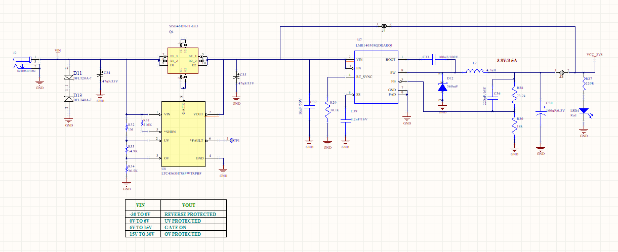
Manjunth : Okay, I have designed this circuit using Webench and verified it.
2. A 0.1uF ceramic is required on the input, in addition to the 10uF you have.
Manjunth : Webench doesn't contain 0.1uF in addition to 10uF, any specific reason for you to say.
3. This capacitor must be placed close to the VIN and GND pins of the device.
Manjunth : Yes Noted
4. The 100uF output capacitor must have low ESR. Two 47uF ceramics can be substituted for the 100uF Al.
Manjunth : I kept same Part number suggest by the Webench with low ESR. I can keep 100uF?
5. Be sure that the inductor and diode are rated for the current limit of the device.
Manjunth : Okay noted, I have followed same as Webench
6. When placing the multiple decoupling capacitors near the input and output pins of an IC, smaller vale capacitor should be placed near the supply pins first or larger value Cap placed near the supply pins?


 and review the same.

