This thread has been locked.

If you have a related question, please click the "Ask a related question" button in the top right corner. The newly created question will be automatically linked to this question.

BQ25713: Thermal optimization design review

Part Number: BQ25713

Hello,

We have developed a charger for 4s battery pack using BQ25713RSNR.The charge current is 2A max with switching frequency of 800kHz.During the operation the inductor is heating to 70C-80C. After review we have considered the following changes.

System setup:
input:12V  output:16.4V   charging current:2Amax   

  •     Inductor with lesser Rdc and higher Isat

              inductor in current design:
                 PN: BWVS008080402R2M00  Rdc:11.5mohms+-30%   Isat:9.2A
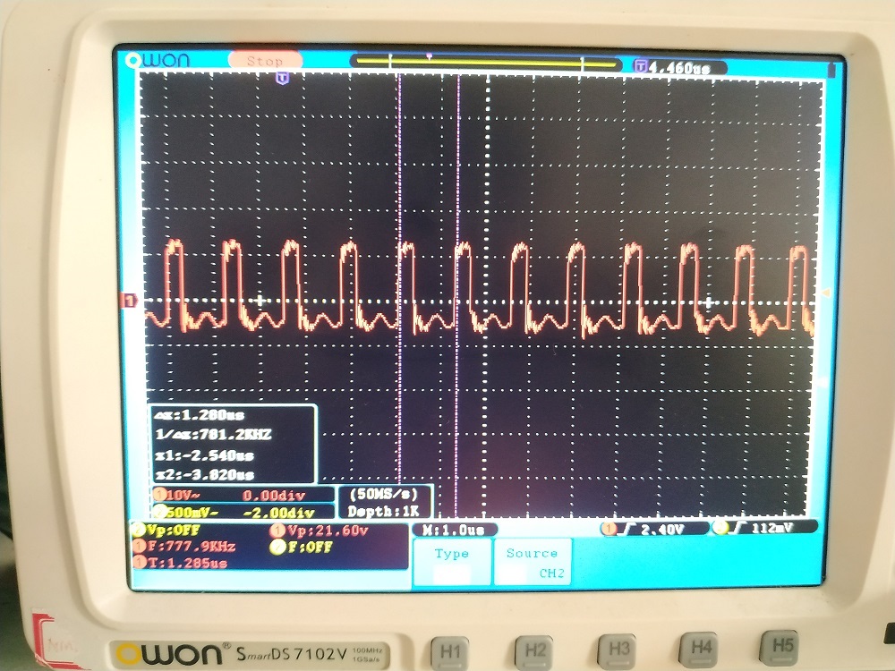
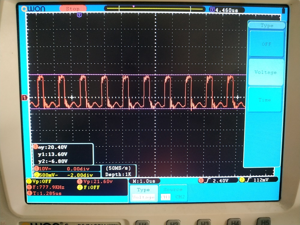
                 Inductor ripple current waveforms picture is provided in the attachment

  •     thermal vias for switching mosfets.

  •     mosfets with lower Qg and Rdson,

                mosfet in current design:
                PN: RQ3E100BNTB  having  Qg=22nC and Rdson:10.4mohms

Kindly review and let us know if we have missed any keypoint for the thermal optimization.

Attachments:

1)schematic

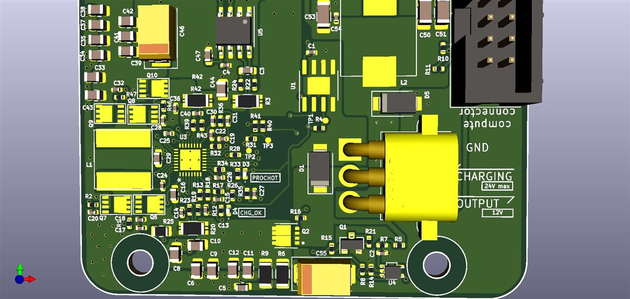
2)PCB layout screenshot with power path

3) voltage waveforms obtained from inductor terminal: inductor current at 2A


5483.file5F65E13A-charger.pdf


  • Hi Kishor,

       If not using CMPIN, ground this pin and float CMPOUT. For thermal optimization, you have correctly addressed a number of key points which is good. You can also focus on keeping the ground plane as uniform as possible and increase the copper area for the ground plane for more effective thermal dissipation.

    From schematic perspective, you have series gate drive resistors for all the switching FET which increases thermal due to gate driver losses. This slows down both turn on and turn off of the switching FET and is not ideal. I would replace these resistors with 0 ohm resistors, and then populate with series resistance as you see fit, depending on EMI.