This thread has been locked.

If you have a related question, please click the "Ask a related question" button in the top right corner. The newly created question will be automatically linked to this question.

TPS63900: High output voltage drop during load transients of 550mA for 10ms/100ms

Part Number: TPS63900
Other Parts Discussed in Thread: TPS63070

We are developing a battery-operated device which detects motion and sends data via LTE-M.
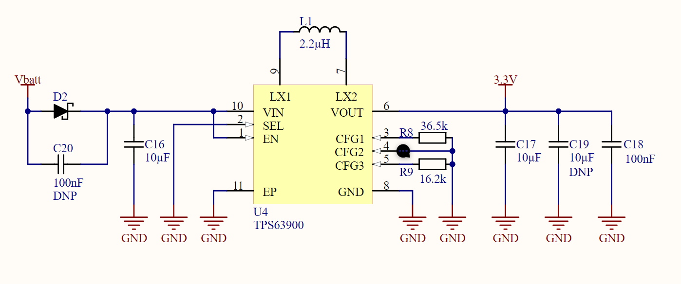
While testing our power supply circuit with the TPS63900 DC-DC converter we noticed some unexpected behavior.
The DC-DC is configured to unlimited current and 3.3V on the output. We use 10uF on the input and output.

There are two issues:
- For 3GPP compliance of our modem we need a stable 3.3V while sending LTE-M messages. We see a voltage drop of approx. 150mV at the output at loads of: 50mA standby current and a load pulse of 550mA for 10ms/100ms. We see more or less the same voltage drop at input voltages from 3.3V to 6V. (We also see the same drop when drawing constant currents of 400mA) The datasheet tells us the maximum pulse current is 1.45A for 1 sec at 1.8V input voltage.

- A min. input voltage of 2.8V at the DC-DC is needed to ensure a 3.0V supply voltage when sending messages. A lower input voltage causes the MCU to constantly reset. The datasheet tells us the min. input voltage is 1.8V.

We also have a question about absolute maximum input voltage. Can we safely use an input voltage of 6.5V for a long periods of time (say 1-2 years)? The datasheet tells us 5.9V is the absolute maximum, but we have tested the device at 8.3V and it still could source multiple current peaks of 1A for 1s. At 8.4V it permanently failed because of the first current peak.

I have added:

  • Detailed test results
  • A picture of our schematic
  • A screenshot of a load test 550mA at 100ms where we configured the DC-DC Vout to 3.6V, Vin 4.5V from a PSU.
What to test How to test Condition(s) Desired results Results Pass/fail
Dropout voltage at different Vin CC Load = 100mA, reduce input voltage until output is 3.2V CC load 100mA. room temperature. Min. Vout of 3.3V at 2.5Vin @ 100mA Vin 2.14V DC-DC shuts off. 2.67V is powers on again. Pass
Absolute Maximum input voltage Increase Vin with 50mV increments from 6V. CC load of 10mA with 10x 1s transients of 1A at every voltage level. Current limit 3.2A, no shotkey diode or capacitor Min. 6.5V 8.3V it succesfully sank 10 load transients. At 8.4V the power circuit died and shorted the Power supply (3.2A) Pass
Output voltage drop Power device with PSU, draw a standby current with the load tester and initiate load transients at different durations. Measure the voltage drop at the output of the DC-DC. Vin 2.5V. Standby current of 50mA. Transient current of 550mA for 1ms, 10ms, 100ms and 1000ms. Min of 3.0V output voltage and message is received at back-end. 2.8V Vin is the min. Semi-pass
Output voltage drop Power device with PSU, draw a standby current with the load tester and initiate load transients at different durations. Measure the voltage drop at the output of the DC-DC. Vin 2.5V. Standby current of 50mA. Transient current of 550mA for 1ms, 10ms, 100ms and 1000ms. Min of 3.3V output voltage and message is received at back-end. even at 6V in the output voltage drops to 3.140V Fail
Efficiency Cut 3V3 trace and measure input current, input voltage, output voltage and output current at different loads. Condition 1. Vout 3.3V ; Iload = 13.4mA ; Pout = 44mW >= 90% Vin = 2.5V ; Iin = 19.5mA Pin = 49mW ; Efficiency = 90% ||| Vin = 3.3V ; Iin = 14.4mA Pin = 47.5mW Efficiency = 92.6% ||| Vin = 4.0V ; Iin = 12.1mA Pin = 48.4mW Efficiency = 90.9% Pass
Quiescent current at different Vin Cut 3V3 trace, no load attached, and measure input current. Vary the input voltage. Vin 2.5V, 3.3V, 4.0V, 5V, 5.5V, 6.0V, 6.5V. <500nA (datasheet claims 75uA load) Vin = 2.5V @ Iq = ~440nA. Vin = 3.3V @ Iq = ~610nA. Vin = 4V @ Iq = 1.2uA. Vin = 5V @ Iq = 1.62uA. Vin = 5.5V @ Iq = 1.85uA. Vin = 6.0V @ Iq = 2.2uA. Vin = 6.5V @ Iq = 2.9uA. Semi-pass
Noise Connect Oscilloscope to Output voltage of DC-DC. 10mV/Div CC load 100mA, Vin 4.5V, 3.3V and 2.5V, at room termperature. <100mV 50mV Pass

  • Hi Tim,

    Here are some explanation about your questions:

    1.1.45 A means peak switching current limit not load current. For Boost condition, average inductor current is above than load current, and peak current of inductor is much higher than average current. So the maximum load current is much less than 1.45A. Though input current is not limited, the peak current can be much larger and reaches limit when load transient because of inrush current. This should be the reason of large voltage drop and 2.8V minimum Vin, you can share the waveform of inductor for better check.

    2. Higher voltage than maximum should not be used. The reliability can not be guaranteed and the device can not work for long time. If you need higher input voltage, TPS63070 can be considered.

    Best Regards,

    Yichen Xu

  • Dear Xu,


    Thank you for your reply.

    1. Can you explain to me if the Y-axis on the graph below corresponds to the load current or that 'Maximum Output Current' explains a different characteristic?

    Perhaps if you have an idea, you could propose a workaround to me on how we could reduce output voltage dropout without replacing the TPS63900?

    2. I understand that TI cannot guarantee reliability above the above absolute maximum input voltage, but do you maybe have information on the amount of lifespan we lose when we use a input voltage of 6.5V? If the lifespan goes from e.g. 10 years to 2 years, we might still be interested.

    Kind regards,

    Tim van Haren

  • Hi Tim,

    1. The graph means the maximum current capacity with different Vin and Vout. I repeated your working condition on our EVM, and it works well. There are two factors affecting your failure. Firstly, did you measure Vin on C16 or just use VBat? There is voltage drop on the cable and D2 between your power supply and real Vin, so the real Vin may be less than 2.5V. Secondly, what inductor did you use? Although the inductance is 2.2uH on your schematic, if the current rating is not big enough it will also cause similar issue. Using L, C in EVM user guide would be fine.

    2. We do not have information like that. It is not recommend. Perhaps this device could work but that device can not. Obviously it is not acceptable.

    Best Regards,

    Yichen Xu

  • Hi Xu,

    Thanks again for your quick response.

    1. We are using the DFE201210S-2R2M=P2. Shouldn't be a problem:

    • 2.2uH with a tolerance of :20%
    • Test frequency: 1MHz
    • Itemp: 1.5A
    • Isat: 2.1A 
    • Res: 0.155Ohm
    • Abs max. voltage: 20 VDC

    "did you measure Vin on C16 or just use VBat?" Both.

    The voltage on the PSU connector and Vin was about the same (40mV drop on the cable when supplied with the PSU). 

    I measured a significant voltage drop on Vin, regardless of type of supply. I tested AA, Li-Ion, Super-cap/LIC and PSU.

    A Super-cap/LIC 340F 4.0V performed better with less drop.

    That's why I think it might has to do with a high inrush current at the input. I tried 20uF input capacitance but the drop didn't decrease significantly and a bigger cap won't fit on our 20x20mm pcb.

    2. I understand, thanks anyway. We are going to do some long duration stress tests on devices with a 6.5V input voltage and see what their lifespan is when we let those devices send a LTE-M message every 30s 1000x. If we have some valuable  information I will update you on that.

    Kind regards,

    Tim van Haren

  • Hi Tim,

    1. Does 'voltage drop on Vin' mean voltage drop between VBat and Vin pin of TPS63900? If yes, the main voltage drop is caused by D2. And I do not think D2 is needed because there is almost no reverse current when the device is working.

    2. Thanks for the test you are going to do. What is your working condition and what kind of feature do you concern? There are buckboost devices with higher input voltage range.

    Best Regards.

    Yichen

  • Hi Tim,

    Long time no hearing from you. I think you have solved your problem. If not, welcome to contact us again~

    Best Regards.

    Yichen

  • Hi Xu,


    I would like to keep this issue open for a bit longer if you don't mind.
    My time was spend on some higher priority tasks so I couldn't find time to test my circuit with the inductor from the eval kit.

    Once I have results from these tests I will report in this thread and you can close it.

    Thanks and kind regards,

    Tim van Haren

  • Hi Tim,

    Sure. Hope to hear good news about your test. Feel free to contact us if you have further questions.

    Best Regards,

    Yichen