This thread has been locked.

If you have a related question, please click the "Ask a related question" button in the top right corner. The newly created question will be automatically linked to this question.

LM5102: LM5102MM power dissipation reducing

Part Number: LM5102
Other Parts Discussed in Thread: LM5041, CSD19535KTT,

Hi,

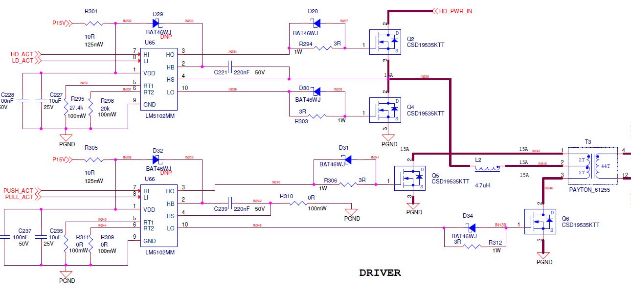
I have a PS design based on LM5041 and LM5102MM as driver.

Switching frequency is 400KHZ. Driver drive CSD19535KTT mosfets (7.9nF).

The LM5102MM is overheating.  I've added optional diodes to decrease power dissipation in the driver, this doesn't help too much.

Can you suggest something with current design?

  • Hello Gleb,

    The file did not properly attach, can you please share the schematic?

    Additionally, what is your VDD voltage and how much gate resistance do you current use? I ask based on the thermal dissipation formula of the IC during the switching transitions of where Psw ~= 2 *VDD * Fsw * Qg * ( 1 / Rgate,total ).

    You may increase your gate resistor which will share the power dissipation away from the driver IC and check whether it is sufficient for your application while considering trade-offs slower rise/fall times at the gate.

    Regards,

    -Mamadou  

  • Thank you very much for such fast response,

    I've attached schematic, hopefully it was attached good now.

    So regarding to your questions:   VDD is connected to 15V through 10R resistor, because 15V is the minimum working voltage for LM5041.

    At 20-28V input power at HD_PWR_IN  the drivers were very hot, but still were running ok, even at 70C ambient temperature.

    But, when input voltage increased to 32V, the drivers were extremely hot and burned. (even at 20C ambient).

    I saw that we have bad package (VSSOP-10) with RθJA=165C/W, we will change it in the future, but for now, I am looking for a temporary solution.

    Installation of optional diodes D29, D32 improve the situation a little bit, but I afraid not enough.

    My question to you is: How do you explain effect of input voltage on drivers, if VDD of drivers is stabilized and doesn't change?

  • Hello Gleb,

    I noticed that the gate charge of the MOSFETs is 78nC with two on each driver for a total of 156nC. The total gate drive power is Qg x VDD x fsw so if the switching frequency is high the gate drive power may be a consideration.

    For your question, with increasing input voltage, the gate charge that is from the gate to drain capacitance of the MOSFET will increase, so the gate drive power does increase with higher MOSFET input voltage. Another consideration, is if the drivers are located close to the MOSFET's and if the MOSFET's are higher temperature with higher input voltage, this can increase the temperature of the driver due to close proximity to the power MOSFET's.

    I would suggest reviewing the LM5102 datasheet sections 8 and 9 to estimate the gate driver power dissipation, and consider a lower thermal resistance package. The DGS package does show much higher thermal resistance than the DPR package.

    Regards,