This thread has been locked.

If you have a related question, please click the "Ask a related question" button in the top right corner. The newly created question will be automatically linked to this question.

TPS23881: About PCB Layout

Part Number: TPS23881

Hi,

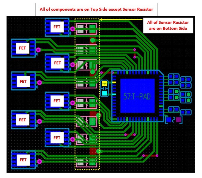
Our customer is working PCB layout and Their PCB size is small and not enough space.

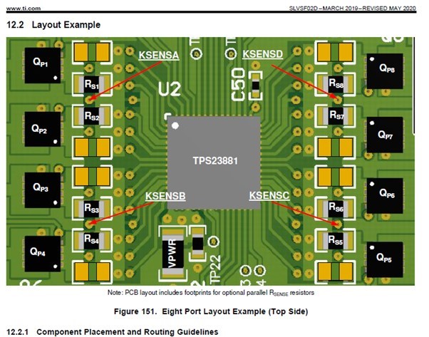
So they can't follow TI PCB Layout Example.

Below is our customer's PCB Layout.

Is there no issue? and Could you please review and guide?

* Customer Layout

* TI Layout Example

Best Regards,

Michael

  • Hi Michael,

    From a sensing prospective, the trace that goes from the sense resistor to SENx pin of the IC should start at the sense resistor and NOT the FET. The ground looks okay on the port side but make sure there is a ground via close to the ground pin of the IC and make sure there is a large ground plane that these gnd vias can connect to.

    From a thermal prospective, be sure there is enough copper on the drain of the FETs and a thick trace from the source to the sense resistor..

    Thanks!