


Other Parts Discussed in Thread: BQ76942, BQSTUDIO, BQ76952
Functions and Variables used in our code to Reading Cell 1 voltage :-
//----Functions & Variable Declaration---------
uint8_t cell1_Volt_Lbyte_Txarr[3],cell1_Volt_Lbyte_Rxarr[3];
uint8_t cell1_Volt_Hbyte_Txarr[3],cell1_Volt_Hbyte_Rxarr[3];
bit Flag_Device_Reset,
Flag_Swap_To_Spi,
Flag_REG0_Config_Enable,
Flag_REG1_Config_Enable;
uint8_t SWAP_SPI_TxArr_L[2],SWAP_SPI_TxArr_H[2],SWAP_SPI_RxArr_L[2],SWAP_SPI_RxArr_H[2];
uint8_t Device_Reset_TxArr_L[2],
Device_Reset_TxArr_H[2],
Device_Reset_RxArr_L[2],
Device_Reset_RxArr_H[2];
uint8_t REG0_TxCmdAdd_L[2],REG0_RxCmdAdd_L[2],
REG0_TxCmdAdd_H[2],REG0_RxCmdAdd_H[2],
REG0_TxDataAdd[1],REG0_RxDataAdd[1],
REG0_TxValue[1],REG0_RxValue[1];
uint8_t REG1_TxCmdAdd_L[2],REG1_RxCmdAdd_L[2],
REG1_TxCmdAdd_H[2],REG1_RxCmdAdd_H[2],
REG1_TxDataAdd[1],REG1_RxDataAdd[1],
REG1_TxValue[1],REG1_RxValue[1];
uint8_t Cell_1_Volt_Lbyte=0,Cell_1_Volt_Hbyte=0;
void ucSPI00_Read_Cell_1_Lbyte_Voltage(void);
void ucSPI00_Read_Cell_1_Hbyte_Voltage(void);
void SWAP_TO_SPI_Communication_Init(void);
void BQ76942_Device_Reset(void);
void REG0_Config_Enable(void);
void REG1_Config_Enable(void);
//---Calling of main function------------------------------
void main(void)
{
PIOR4 = 0x00U;
SELLOSC = 1U;
MDIV = 0x00;
SELPLL = 0U;;
CMC = 0x00; //X1 & X2 pins of oscillator as INPUT; port pins.
CKC = 0x00; //SELECT INTERNAL HIGH SPEED OSCILLATOR.
CSC = 0xC0; //EXTERNAL OSCILLATOR X1-X2 AND XT1-XT2 STOPPED,INTERNAL HIGH SPEED OSCILLATOR OPERATING.
HOCODIV = 0x00; //NO FREQUENCY DIVISION --- Bus Clock = 24MHz
CRC0CTL = 0x00;
IAWCTL = 0x00;
vMain_PowerOnInit();
EI();
//-------------------------------------------------------------------------------
//---Date 03-12-2020 @ 016:51 PM
//------Device Reset commmand=0x0012
Device_Reset_TxArr_L[0]=0xBE;//--(R/W bit=1 for Write)+0x3E=0xBE
Device_Reset_TxArr_L[1]=0x12;//--Lower byte =0x12
Device_Reset_TxArr_H[0]=0xBF;//--(R/W bit=1 for Write)+0x3F=0xBF
Device_Reset_TxArr_H[1]=0x00;//--Higher Byte=0x00
//-----------------------------------------------------------------------------
//--SWAP TO SPI Command =0x7C35-------
SWAP_SPI_TxArr_L[0]=0xBE;//--(R/W bit=1 for Write)+0x3E=0xBE
SWAP_SPI_TxArr_L[1]=0x35;//Lower Byte=0x35
SWAP_SPI_TxArr_H[0]=0xBF;//--(R/W bit=1 for Write)+0x3F=0xBF
SWAP_SPI_TxArr_H[1]=0x7C;//Higher Byte=0x7C
//-----------------------------------------------------------------------------
//---REG0 Config Enable : Address=0x921B, Data =0x01(REG0_EN bit =1)
//---Addres write(0x921B)
REG0_TxCmdAdd_L[0]=0xBE;//--(R/W bit=1 for Write)+0x3E=0xBE
REG0_TxCmdAdd_L[1]=0x1B;//Lower byte=0x1B
REG0_TxCmdAdd_H[0]=0xBF;//--(R/W bit=1 for Write)+0x3F=0xBF
REG0_TxCmdAdd_H[1]=0x92;//Higher byte=0x92
//--Data addr write at 0x40=0x01
REG0_TxDataAdd[0]=0xC0;//--(R/W bit=1 for Write)+0x40=0xC0(To write value @ 0x40)
//--Value write
REG0_TxValue[0]=0x01;//Data =0x01(REG0_EN bit =1)
//-----------------------------------------------------------------------------
//--REG1=3.3V Enable : Address=0x921A, Data=0x0D(3.3 volt )[REG1V_2=1,REG1V_1=1,REG1V_0=0, REG0_EN bit =1]
//---Addres write(0x921A)
REG1_TxCmdAdd_L[0]=0xBE;//--(R/W bit=1 for Write)+0x3E=0xBE
REG1_TxCmdAdd_L[1]=0x1A;//Lower byte=0x1A
REG1_TxCmdAdd_H[0]=0xBF;//--(R/W bit=1 for Write)+0x3F=0xBF
REG1_TxCmdAdd_H[1]=0x92;//Higher byte=0x92
//--Data addr write at 0x40=0x0D
REG1_TxDataAdd[0]=0xC0;//--(R/W bit=1 for Write)+0x40=0xC0(writing value @ 0x40)
//--Value write
REG1_TxValue[0]=0x0D;//--Data =0x0D(REG1V_2=1,REG1V_1=1,REG1V_0=0, REG0_EN bit =1)
//-----------------------------------------------------------------------------
//--- cell 1 Lbyte Reading ----
cell1_Volt_Lbyte_Txarr[0]=0x14;//0x14 location Read
cell1_Volt_Lbyte_Txarr[1]=0xFF;
//---Cell 1 Hbyte Reading -----
cell1_Volt_Hbyte_Txarr[0]=0x15;//0x15 location Read
cell1_Volt_Hbyte_Txarr[1]=0xFF;
Flag_Device_Reset=1;
Flag_Swap_To_Spi=1;
Flag_REG0_Config_Enable=1;
Flag_REG1_Config_Enable=1;
while(1)
{ //main while start
//-----------------------------BQ76942 Device Initialization-----------------------------------------------------------------------------
while(Flag_Device_Reset) //--Send Device Reset commmand-->>0x0012 till correct value return
{
BQ76942_Device_Reset();
if((Device_Reset_TxArr_L[0]==Device_Reset_RxArr_L[0])&&(Device_Reset_TxArr_H[0]==Device_Reset_RxArr_H[0]))//Checking device reset
Flag_Device_Reset=0;
}
while(Flag_Swap_To_Spi)//-Send SWAP to spi Communication command-->>0x7C35 till correct value returns
{
SWAP_TO_SPI_Communication_Init();
if((SWAP_SPI_TxArr_L[0]==SWAP_SPI_RxArr_L[0])&&(SWAP_SPI_TxArr_H[0]==SWAP_SPI_RxArr_H[0]))//Checking Device swaping to SPI
Flag_Swap_To_Spi=0;
}
while(Flag_REG0_Config_Enable) //Send REG0 Enable command-->>value=0x01(REG0_EN bit =1) at REG0 config at Address=0x921B
{
REG0_Config_Enable();
if((REG0_TxCmdAdd_L[0]==REG0_RxCmdAdd_L[0])&&(REG0_TxCmdAdd_H[0]==REG0_RxCmdAdd_H[0]))//Checking REG0 Enable command
Flag_REG0_Config_Enable=0;
}
while(Flag_REG1_Config_Enable)//Send REG1=3.3V Enable : Address=0x921A, Data=0x0D(3.3 volt )[REG1V_2=1,REG1V_1=1,REG1V_0=0, REG0_EN bit =1]
{
REG1_Config_Enable();
if((REG1_TxCmdAdd_L[0]==REG1_RxCmdAdd_L[0])&&(REG1_TxCmdAdd_H[0]==REG1_RxCmdAdd_H[0]))//Checking REG1 Enable command
Flag_REG1_Config_Enable=0;
}
//----------------------------------------------------------------------------------------------------------------------------------
//----Cell 1 Voltage Reading at 0x14 and 0x15 location
while(1) //--Continous reading of Cell 1 voltage Lower byte
{
ucSPI00_Read_Cell_1_Lbyte_Voltage();// Read Cell_1 voltage lower byte----Send at MOSI (0x14 ,0xFF)
if(cell1_Volt_Lbyte_Txarr[0]==cell1_Volt_Lbyte_Rxarr[0])//Voltage read when (MOSI=0x14 and MISO=0x14)
{
Cell_1_Volt_Lbyte=cell1_Volt_Lbyte_Rxarr[1];
break;
}
}
while(1)//--Continous reading of Cell 1 voltage Higher byte
{
ucSPI00_Read_Cell_1_Hbyte_Voltage();// Read Cell_1 voltage of Higher byte
if(cell1_Volt_Hbyte_Txarr[0]==cell1_Volt_Hbyte_Rxarr[0])//Voltage read when (MOSI=0x15 and MISO=0x15)
{
Cell_1_Volt_Hbyte=cell1_Volt_Hbyte_Rxarr[1];
break;
}
}
//------------------------------------------------------------------------------------------------------------------------
}//main while end
}
//----------------Function Definitions ------------------------------------------------------------------
void REG1_Config_Enable(void)
{
//---Enable REG1 Config: Write value=0x0D(REG1V_2=1,REG1V_1=1,REG1V_0=0, REG0_EN bit =1) at REG1 config Address=0x921A
ucSPI00_ReadWriteData(1,(uint8_t*)®1_TxCmdAdd_L[0],1,(uint8_t*)®1_RxCmdAdd_L[0]); //Write command Addr=0xBE(W=1+0x3E ,write process)
ucSPI00_ReadWriteData(1,(uint8_t*)®1_TxCmdAdd_L[1],1,(uint8_t*)®1_RxCmdAdd_L[1]); //Write REG0 LByte Addr=0x1A
ucSPI00_ReadWriteData(1,(uint8_t*)®1_TxCmdAdd_H[0],1,(uint8_t*)®1_RxCmdAdd_H[0]); //Write command Addr=0xBF(W=1+0x3F ,write process)
ucSPI00_ReadWriteData(1,(uint8_t*)®1_TxCmdAdd_H[1],1,(uint8_t*)®1_RxCmdAdd_H[1]); //Write REG0 HByte Addr=0x92
ucSPI00_ReadWriteData(1,(uint8_t*)®1_TxDataAdd[0],1,(uint8_t*)®1_RxDataAdd[0]); //Write Data Addr=0xC0(W=1+0x40 ,write value @ 0x40)
ucSPI00_ReadWriteData(1,(uint8_t*)®1_TxValue[0],1,(uint8_t*)®1_RxValue[0]); //Write value=0x0D (REG1V_2=1,REG1V_1=1,REG1V_0=0, REG0_EN bit =1) at 0xC0
}
void REG0_Config_Enable(void)
{
//---Enable REG0 Config: Write value=0x01(REG0_EN bit =1) at REG0 config Address=0x921B
ucSPI00_ReadWriteData(1,(uint8_t*)®0_TxCmdAdd_L[0],1,(uint8_t*)®0_RxCmdAdd_L[0]); //Write command Addr=0xBE(W=1+0x3E ,write process)
ucSPI00_ReadWriteData(1,(uint8_t*)®0_TxCmdAdd_L[1],1,(uint8_t*)®0_RxCmdAdd_L[1]); //Write REG0 LByte Addr=0x1B
ucSPI00_ReadWriteData(1,(uint8_t*)®0_TxCmdAdd_H[0],1,(uint8_t*)®0_RxCmdAdd_H[0]); //Write command Addr=0xBF(W=1+0x3F ,write process)
ucSPI00_ReadWriteData(1,(uint8_t*)®0_TxCmdAdd_H[1],1,(uint8_t*)®0_RxCmdAdd_H[1]); //Write REG0 HByte Addr=0x92
ucSPI00_ReadWriteData(1,(uint8_t*)®0_TxDataAdd[0],1,(uint8_t*)®0_RxDataAdd[0]); //Write Data Addr=0xC0(W=1+0x40 ,write value @ 0x40)
ucSPI00_ReadWriteData(1,(uint8_t*)®0_TxValue[0],1,(uint8_t*)®0_RxValue[0]); //Write value=0x01(REG0_EN bit =1) at 0xC0
}
void BQ76942_Device_Reset(void)
{ //------Device Reset commmand 0x0012
ucSPI00_ReadWriteData(1,(uint8_t*)&Device_Reset_TxArr_L[0],1,(uint8_t*)&Device_Reset_RxArr_L[0]); //Write command Addr=0xBE(W=1+0x3E ,write process)
ucSPI00_ReadWriteData(1,(uint8_t*)&Device_Reset_TxArr_L[1],1,(uint8_t*)&Device_Reset_RxArr_L[1]); //Write command Addr=0x12
ucSPI00_ReadWriteData(1,(uint8_t*)&Device_Reset_TxArr_H[0],1,(uint8_t*)&Device_Reset_RxArr_H[0]); //Write command Addr=0xBF(W=1+0x3F ,write process)
ucSPI00_ReadWriteData(1,(uint8_t*)&Device_Reset_TxArr_H[1],1,(uint8_t*)&Device_Reset_RxArr_H[1]); //Write command Addr=0x00
}
void SWAP_TO_SPI_Communication_Init(void)
{ //----SWAP TO SPI COMMAND=0x7C35
ucSPI00_ReadWriteData(1,(uint8_t*)&SWAP_SPI_TxArr_L[0],1,(uint8_t*)&SWAP_SPI_RxArr_L[0]); //Write command Addr=0xBE(W=1+0x3E ,write process)
ucSPI00_ReadWriteData(1,(uint8_t*)&SWAP_SPI_TxArr_L[1],1,(uint8_t*)&SWAP_SPI_RxArr_L[1]); //Write command Addr=0x35
ucSPI00_ReadWriteData(1,(uint8_t*)&SWAP_SPI_TxArr_H[0],1,(uint8_t*)&SWAP_SPI_RxArr_H[0]); //Write command Addr=0xBF(W=1+0x3F ,write process)
ucSPI00_ReadWriteData(1,(uint8_t*)&SWAP_SPI_TxArr_H[1],1,(uint8_t*)&SWAP_SPI_RxArr_H[1]); //Write command Addr=0x7C
}
void ucSPI00_Read_Cell_1_Lbyte_Voltage(void)
{
ucSPI00_ReadWriteData(1,(uint8_t*)&cell1_Volt_Lbyte_Txarr[0],1,(uint8_t*)&cell1_Volt_Lbyte_Rxarr[0]);//Write command Addr=0x14 //cell volt 1 Lbyte
ucSPI00_ReadWriteData(1,(uint8_t*)&cell1_Volt_Lbyte_Txarr[1],1,(uint8_t*)&cell1_Volt_Lbyte_Rxarr[1]);//Write command Addr=0xFF//dummy byte
}
void ucSPI00_Read_Cell_1_Hbyte_Voltage(void)
{
//---Cell 1 Hbyte-----
cell1_Volt_Hbyte_Txarr[0]=0x15;//0x15 location Read
cell1_Volt_Hbyte_Txarr[1]=0xFF;
ucSPI00_ReadWriteData(1,(uint8_t*)&cell1_Volt_Hbyte_Txarr[0],1,(uint8_t*)&cell1_Volt_Hbyte_Rxarr[0]);//Write command Addr=0x15//cell volt 1 Hbyte
ucSPI00_ReadWriteData(1,(uint8_t*)&cell1_Volt_Hbyte_Txarr[1],1,(uint8_t*)&cell1_Volt_Hbyte_Rxarr[1]);//Write command Addr=0xFF//dummy byte
}
/**********************************************************************************
Name : ucSPI00_ReadWriteData
Parameters : pTxBuf : Starting Address of Tx Buffer
: ucTxByte: No of Byte to be Tx
: pRxBuff : Rx Buffer Address
Returns : None
Description : To Send & Receive Data on SPI Bus-CH0
***********************************************************************************/
uint8_t ucSPI00_ReadWriteData(uint8_t ucDevID,uint8_t *pTxBuf, uint8_t ucTxByte, uint8_t *pRxBuf)
{
if (ucTxByte < 1U)
{
return 0;
}
else
{
ucSPI_CommDevID = ucDevID;
ucSPI_TxByteCount = ucTxByte;
pSPI_TxAdd = pTxBuf;
if(ucSPI_CommDevID==defSPI0_DevID_BMS)
{
pSPI01_RxAdd = pRxBuf;
pSPI00_RxAdd = ucSPI_DummyByte;
}
else
{
if(ucSPI_CommDevID==defSPI0_DevID_Flash)
{
pSPI00_RxAdd = pRxBuf;
pSPI01_RxAdd = ucSPI_DummyByte;
}
}
CSIMK00 = 1U; // Disable Interrupt
SDR00L = *pSPI_TxAdd; // Send First Byte
pSPI_TxAdd++;
ucSPI_TxByteCount--;
CSIMK00 = 0U; // Enable INTCSI00 interrupt
}
return 1;
}
/**********************************************************************************
Name : vSPI_ISR_SPI00
Parameters : None
Returns : None
Description : ISR to Transmit & Data on SPI Bus-CH0
***********************************************************************************/
__interrupt static void vSPI_ISR_SPI00(void)
{
*pSPI00_RxAdd = SDR00L;
pSPI00_RxAdd++;
if (ucSPI_TxByteCount != 0U)
{
SDR00L = *pSPI_TxAdd;
pSPI_TxAdd++;
ucSPI_TxByteCount--;
}
else
{
if (ucSPI_TxByteCount == 0U)
{
bSPI_TxStatusFlag = HIGH;
}
}
}
Hi TI Forum Team,
I am working on BQ76942 EVM board. Actually I want to SPI communication of BQ76942 Device with our Renesas RL78/F13(R5F10BGE) LQFP-48pin microcontroller over SPI00 Chanel.
Hardware connection Details given below how BQ76942 BMS is connected with RL78/F13(R5F10BGE) Microcontroller for SPI00 connection.
BQ76942 Pins ---------------->> RL78/F13(R5F10BGE) Pins
(1 ) SPI_SCLK(26-pin)---->>P1.7(SCK00)
(2) SPI_MISO(27-pin)----->>P1.6(SI00)
(3) SPI_MOSI(28-pin)----->>P1.5(SO00)
(4) SPI_CS(29-pin)------->> P3.0(SSI00)
My Problem points:-
(1) When I sent these following command sequence to Read the Cell 1 Voltage which is at location 0x14 and 0x15 of BQ76941 RAM location. I did not get the value of Cell 1 voltage reading,
some time we get 0x00 and 0xFF from both location.
(2) please look my command sequence or is it right command that I have sent for Cell 1 voltage reading?
(3) If the above command and its sequence is not right way please let me know both right command and its sequence for voltage reading of Cell 1
Note:- (1.) I have Keep the SPI Communication Frequency at 2MHz from controller side , as stated in SPI supporting speed in BQ76942 data sheet.
(2.) I have keep the same BQ76942 SPI Interface logic operates with Clock polarity(CPOL=0) and clock Phase(CPHA=0) as mentioned clock and data timing diagram in BQ76942 data sheet as well as in Microcontroller (R5F10BGE) is which is covered in type4 which highlight in Screen shot attached with it.
BQ76942 SPI Timing Diagram
Microcontroller RL78/R5F10BGE SPI mode Timing diagram
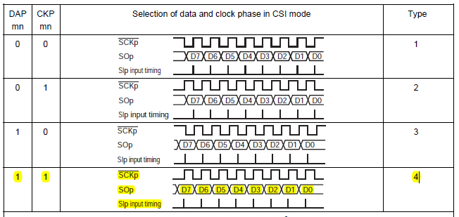
(3) As per above both Timing Diagram Microcontroller Timing Diagram Type4 is equivalent to BQ76942 CPOL=0 and CPHA=0 . so we have keep mode =Type4 in our Microcontroller side.
(4) These above setting I have maintained in our source code in SPI communication from Microcontroller side.
Our command & its sequence what we implement in our source code For Cell 1 Voltage Reading :-
(1)------Device Reset commmand=0x0012
Device_Reset_TxArr_L[0]=0xBE;//--(R/W bit=1 for Write)+0x3E=0xBE
Device_Reset_TxArr_L[1]=0x12;//--Lower byte =0x12
Device_Reset_TxArr_H[0]=0xBF;//--(R/W bit=1 for Write)+0x3F=0xBF
Device_Reset_TxArr_H[1]=0x00;//--Higher Byte=0x00
//-----------------------------------------------------------------------------
(2)--SWAP TO SPI Command =0x7C35-------
SWAP_SPI_TxArr_L[0]=0xBE;//--(R/W bit=1 for Write)+0x3E=0xBE
SWAP_SPI_TxArr_L[1]=0x35;//Lower Byte=0x35
SWAP_SPI_TxArr_H[0]=0xBF;//--(R/W bit=1 for Write)+0x3F=0xBF
SWAP_SPI_TxArr_H[1]=0x7C;//Higher Byte=0x7C
//-----------------------------------------------------------------------------
(3)---REG0 Config Enable : Address=0x921B, Data =0x01(REG0_EN bit =1)
//---Addres write(0x921B)
REG0_TxCmdAdd_L[0]=0xBE;//--(R/W bit=1 for Write)+0x3E=0xBE
REG0_TxCmdAdd_L[1]=0x1B;//Lower byte=0x1B
REG0_TxCmdAdd_H[0]=0xBF;//--(R/W bit=1 for Write)+0x3F=0xBF
REG0_TxCmdAdd_H[1]=0x92;//Higher byte=0x92
//--Data addr write at 0x40=0x01
REG0_TxDataAdd[0]=0xC0;//--(R/W bit=1 for Write)+0x40=0xC0(To write value @ 0x40)
//--Value write
REG0_TxValue[0]=0x01;//Data =0x01(REG0_EN bit =1)
//-----------------------------------------------------------------------------
(4)--REG1=3.3V Enable : Address=0x921A, Data=0x0D(3.3 volt )[REG1V_2=1,REG1V_1=1,REG1V_0=0, REG0_EN bit =1]
//---Addres write(0x921A)
REG1_TxCmdAdd_L[0]=0xBE;//--(R/W bit=1 for Write)+0x3E=0xBE
REG1_TxCmdAdd_L[1]=0x1A;//Lower byte=0x1A
REG1_TxCmdAdd_H[0]=0xBF;//--(R/W bit=1 for Write)+0x3F=0xBF
REG1_TxCmdAdd_H[1]=0x92;//Higher byte=0x92
//--Data addr write at 0x40=0x0D
REG1_TxDataAdd[0]=0xC0;//--(R/W bit=1 for Write)+0x40=0xC0(writing value @ 0x40)
//--Value write
REG1_TxValue[0]=0x0D;//--Data =0x0D(REG1V_2=1,REG1V_1=1,REG1V_0=0, REG0_EN bit =1)
//-----------------------------------------------------------------------------
(5)--- cell 1 Lbyte Reading ----
cell1_Volt_Lbyte_Txarr[0]=0x14;//0x14 location Read
cell1_Volt_Lbyte_Txarr[1]=0xFF;
(6)---Cell 1 Hbyte Reading -----
cell1_Volt_Hbyte_Txarr[0]=0x15;//0x15 location Read
cell1_Volt_Hbyte_Txarr[1]=0xFF;
//------------------------------------------------------------------------------
Please let me know where I am wrong so that SPI Communication b/w BQ76942 and R5F10BGE controller not happening.
Your co-operation will be Appreciable.
Thanks & Regards
Pankaj Kumar
