This thread has been locked.

If you have a related question, please click the "Ask a related question" button in the top right corner. The newly created question will be automatically linked to this question.

LM7480-Q1: Design issue

Part Number: LM7480-Q1


Hi 

We are having some issues with LM74800 (we are using PLM74800QDRRRQ1 samples that we received in the last month)

I have inserted 2 schematics. The second is a "zoom in" of the LM74800 schematic connectivity. The first is that of the immediate

circuitry in the vicinity to the LM74800.

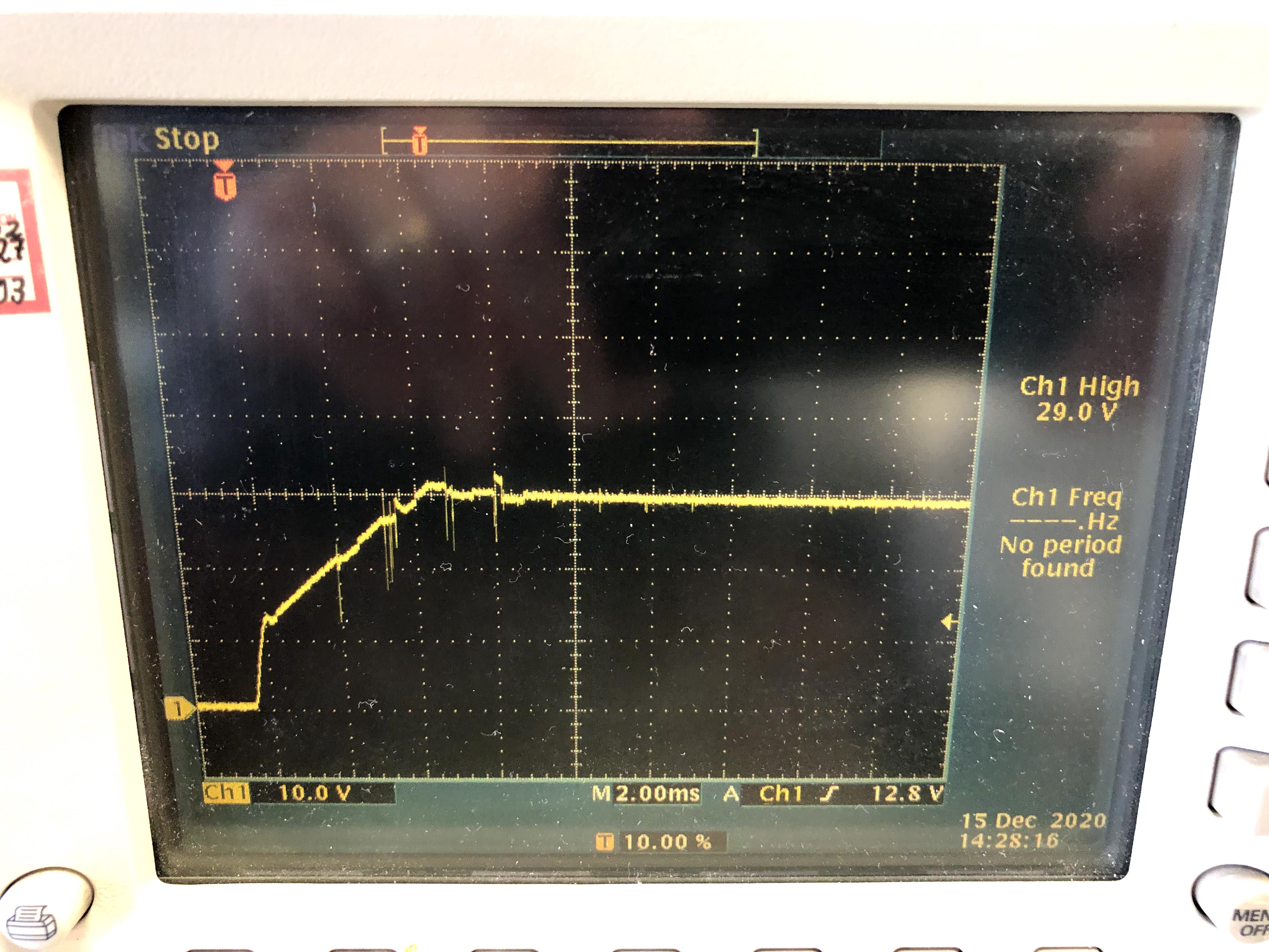
We have connected up the LM74800Q, as illustrated below, to a 24V bench power supply

The load capacitance is in the order of 210uF. The load current is low at present (around 1A) 

Q33 and Q32 are Vishay SQJ402EP.  

We have received 5 prototype boards, and so far either the LM74800 or the FETs have blown on 4 of the units, we are in the process of determining what has blown.

We are holding off from further powering up the only good unit until we can get a better understanding of what might be happening. 

Four units powered up successfully first time, and one did not. After several power-on's the circuitry started to fail on 2 of the units. We modified one of the units so that

EN was driven directly from VIN_FUSE but it eventually failed.

Our application is an "always on ideal diode with the H-gate FET for protection e.g. inrush, overvoltage etc. We believe we have connected up the

device correctly but could someone please verify that we have not made some error.

We have bypassed the ideal diode circuit all together and have no adverse issues with the rest of the circuitry in this design.

One thing that I fail to understand is if the D FET and H FET are enabled by EN, how does connecting EN to Cathode of the diode (in this common drain configuration) 

ensure that the D FET is enabled on power on.

Any thoughts, comments, suggestions etc. would be much appreciated.

Regards

Finbarr

  • Hi Finbarr,

    Thanks for reaching out to us. Let me review your schematics and get back to you by coming Tuesday. 

  • Hi Finbarr,

    The schematic connections look good to me. You can verify your component selection as per section '10.2.3 Detailed Design Procedure' of the datasheet. 

    Regarding your question on EN/UVLO signal, the body diode of Q33 will provide voltage to the common drain point (when DGATE is pulled low) from which the EN/UVLO resistor divider is power up.

    Have you captured any startup waveforms (similar to Figure 10-7 and 10-8) when you first powered up the device ?

    For you information, this device has been released to market now and you can order the final silicon from www.ti.com/.../LM7480-Q1

  • Hi Praveen

    I am not sure how to attach jpeg files as opposed to clogging up this window. But below I am attaching the waveforms that we captured BEFORE we killed the last working unit. 

    Note : we removed the 2 X 100uF capacitors 

    The attachments are in the following order.

    CH1_ID_C_REF_VOUT.jpg  ( ID_C with respect to VIN_IN_HF_In relation to the schematic I sent previously) 

    CH1_VIN_REF_ID_C.jpg (VIN_FUSE with respect to IC_C In relation to the schematic I sent previously)

    ID_DGATE#1.jpg (DGATE output , ID_DGATE output In relation to the schematic I sent previously) 

    ID_DGATE#2.jpg ( stady state DGATE output (if you could call it steady state) , ID_DGATE output In relation to the schematic I sent previously) 

    ID_HGATE.jpg (HGATE output , ID_HGATE output In relation to the schematic I sent previously) 

    VS.jpg (VS input , VS input In relation to the schematic I sent previously) 

    As you ca see there is some very strange behaviour especially on DGATE and HGATE. Any thought or comments are welcome. 

    Regards

    Finbarr

  • Hi Finbarr,

    Thanks for sharing more details. I will review and get back to you with my comments by 23rd Dec.

  • Hi Finbarr,

    It is very difficult to relate the signals in the images with the text that you have written as the images do not have the file name that you have mentioned.

    Can you please attach  document like ppt or excel with all the waveforms with their description of each signals and the condition at which the waveforms were captured. 

    I would be interested to see startup waveforms like below,