This thread has been locked.

If you have a related question, please click the "Ask a related question" button in the top right corner. The newly created question will be automatically linked to this question.

TPS61235P: Switching noise on Boost Converter output

Part Number: TPS61235P

Hello all,

I am facing a problem with the TSP61235PWRLT boost converter IC. I am getting desired voltage (5.15v) on the output side of boost converter but it includes switching frequency. Even after connecting appropriate components I am getting switching frequency (1MHz) on the output side.

Please consider the following schematic and layout for review.

R52 “0 Ohm” resistor is kept DNP.


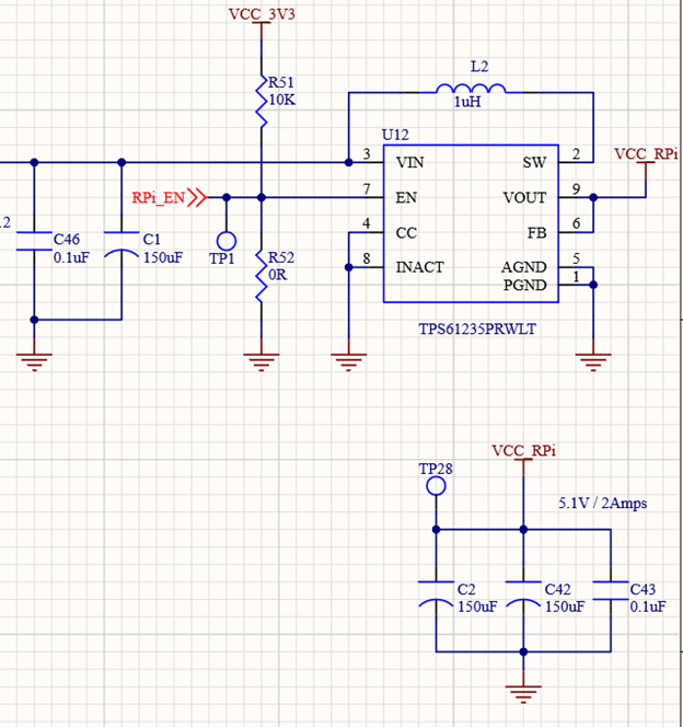
Following are the part number of capacitor and inductor used in boost converter.

  1. Inductor
    1. 1uH – SRN6045TA-1R0Y
  2. Capacitor
    1. 150uF – TSPD157K010S0100 (Both on input and output side)
    2. 0.1uF - CC0402KRX7R7BB104 (Both on input and output side)

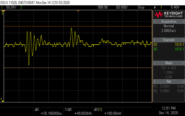
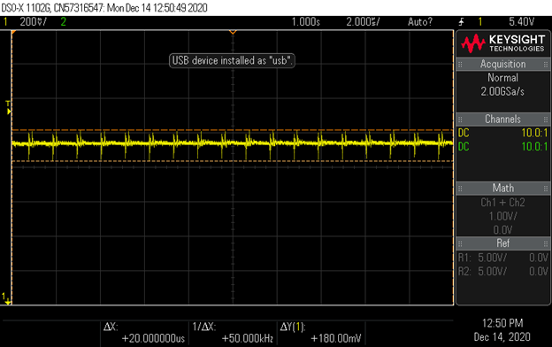
I have attached output images of boost converter for your reference.

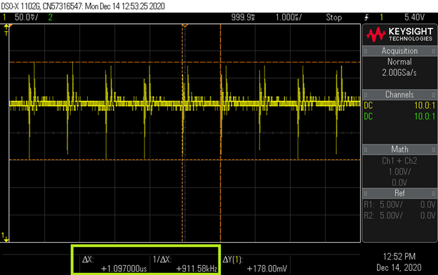
The peak to peak voltage is 178mv and frequency is 911.58 KHz.

Following are the few images of output waveform of boost converter.


  • Hi Peter,

    Sorry I can't see your pictures. Could you share it again?

  • Hello Mr. Zack Liu,

    Thanks for your response.

    I have re-uploaded the images please check.

  • Hi Peter,

    Are C2 and C42 aluminum electrolytic capacitors? Normally aluminum electrolytic capacitors have big ESR, larger than 100mohm. Please solder two 10uF ceramic capacitor close to IC Vout pin and GND pin to reduce the output voltage ripple.

  • Hello Mr. Zack Liu,

    Thanks one again for you response.

    The capacitor C2 and C42 are tantalum capacitor.

    Yes I tried connecting 10uF capacitors on the output side of boost IC after using following software which shows 1Mhz as a resonant frequency for 10uF.

    But still it didn't change anything on output side, I got same response. I also tried a capacitor bank of few MLCC like 1uF, 10uF and 22uF  to create a broad valley so as to provide lower impedance to 1MHz frequency but it didn't work.

    I have also followed the guidelines mention in the datasheet for the layout. 

    Let me know your point of view on this. if there is any other approach to resolve this issue please suggest.

  • Hi Peter,

    1. The output voltage ripple include two parts: 1. Switching frequency ripple, which normally could be reduced with ceramic capacitors because ceramic capacitor has lower ESR. 2. Switching noise. Place the ceramic capacitor close to IC to decrease the parasitic inductance, as well as switching noise.

    2. You can place a ferrite bead at output to filter the switching noise.

    3. Use minimum loop method to measure the output voltage ripple.