A related question is a question created from another question. When the related question is created, it will be automatically linked to the original question.
If you have a related question, please click the "Ask a related question" button in the top right corner. The newly created question will be automatically linked to this question.
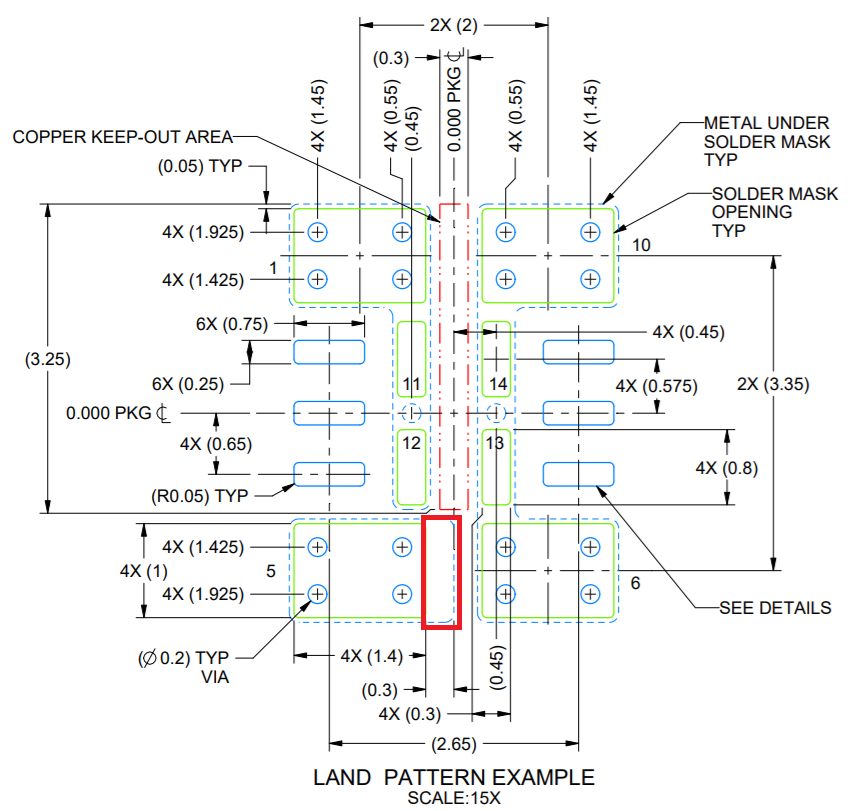
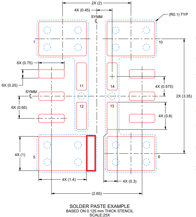
Could you comment whether the extended land pattern and solder paste design of PIN5 is necessary? Thanks! The PCB layout engineers of my customer have some concern on the clearance between PIN5 & PIN6.
Let me check on the reason for making pin 5's land pad larger. It will likely be next week before I can give an answer.
I calculate a pad separation of 250 um between pin 5 and pin 6. Does this match what you calculate? How is this an issue? (I think there is less separation between pins 5 and 12, for example.)
I confirmed that you can choose to not extend pin 5's pad so close to pin 6, if you need to. In most applications, pin 5 is connected to a large copper pour to carry the output current. So, you will likely have copper there anyways from the Vout plane.
I am still curious what issue the spacing between pin 5 and 6 caused for you?