This thread has been locked.

If you have a related question, please click the "Ask a related question" button in the top right corner. The newly created question will be automatically linked to this question.

TPS43061: Efficiency, sub harmonics

Part Number: TPS43061
Other Parts Discussed in Thread: LM5155

Hoping you can give me a hint.

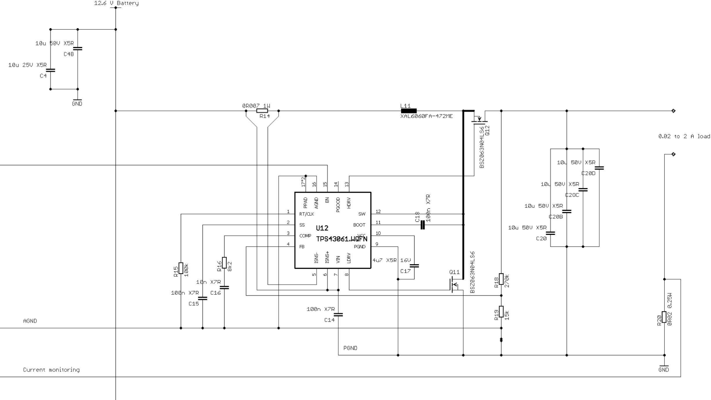
I used Webench and the TPS4306x design spreadsheet for guidance. I did what I think is a good layout (not my first switcher layout).

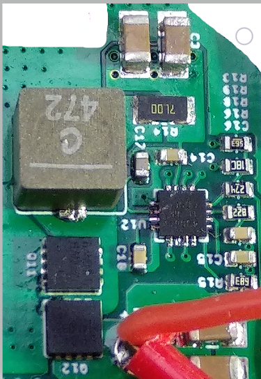
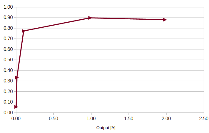
Switch node, current sense, hi drive and lo drive all scope good, up to ~66% output anyway. Vin, Vcc are stable.

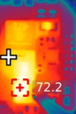
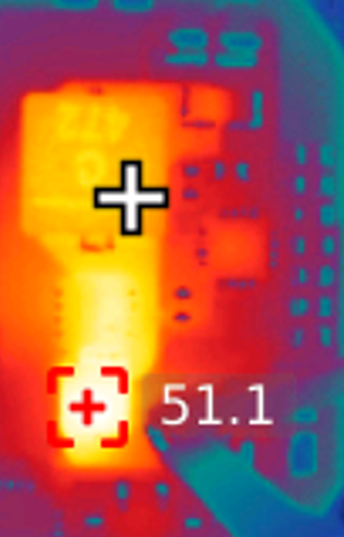
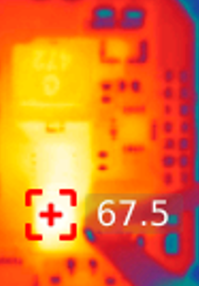
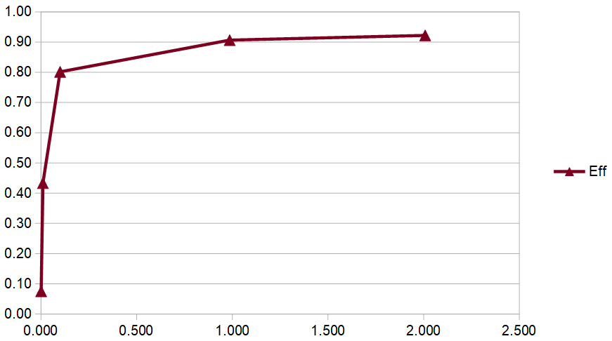
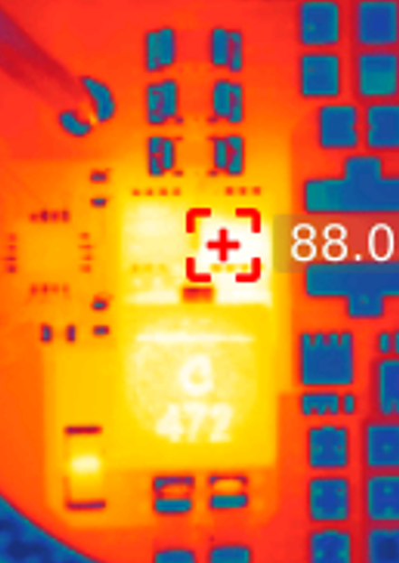
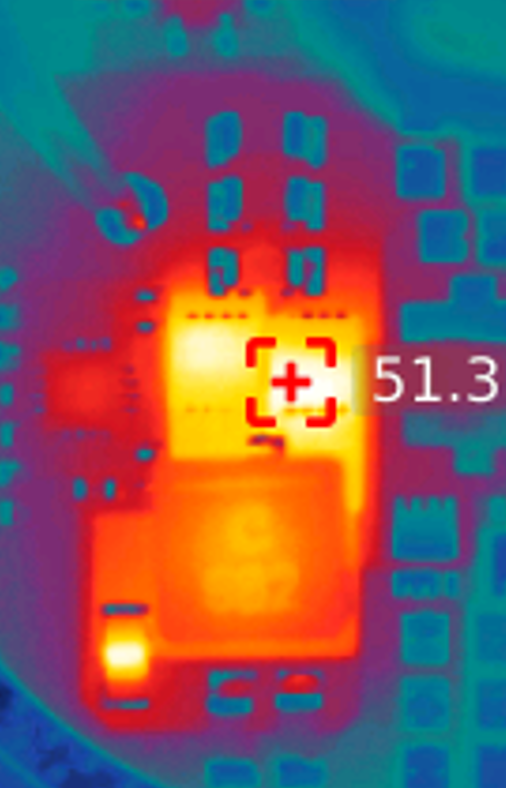
But I only get 88% efficiency and some sub-harmonics above 66% output.

The harmonics goes away if I add output capacitance. But the efficiency does not improve. The resulting heat is a show-stopper for the application.

Where should I look?

Details:

10-12 V in, 27.5 V 0-2 A out. Output ripple spec is not very important.

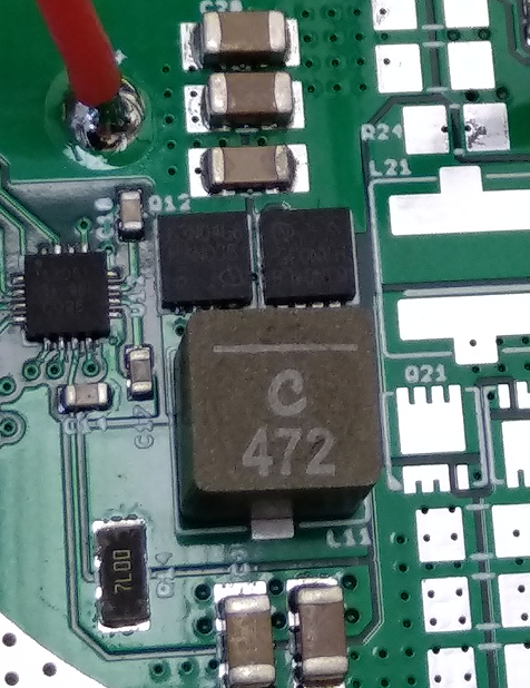
4-layer board with tight layout, tight loops for high and low drives.

Fs = 820 kHz (68 kohm)

Inductor is an XAL6060 4.7 uH (14.4 mohm)

7 mohm current sense

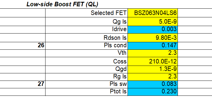
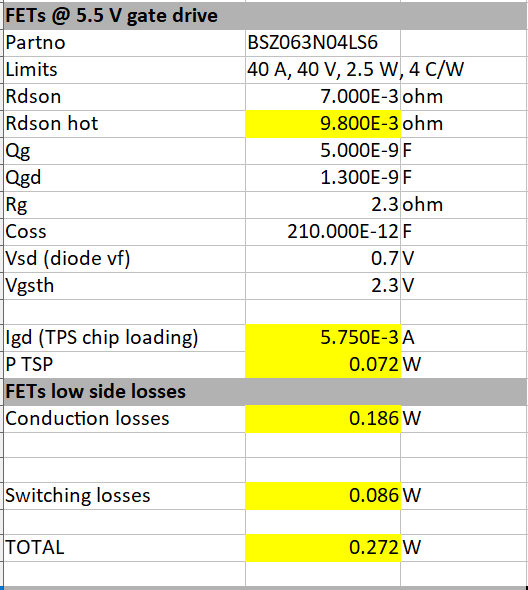
FETs are Infineon BSZ063N04LS6 (6.3 mohm, ~6 nC)

Cin = 2x 1206 Samsung 10 uF 50 V X5R

Cout = same

No RC filtering for the current sense (board space is tight).

Aiming for 94-95% efficiency.

Thanks!

  • Hello discrete,

    I would recommend to check which components are getting hot and check these first.

  • Hi Brigitte,

    Thank you for getting back to me.

    There are some thermal images below. At <66% loading QH seems to run the hottest, at full load it is QL.

    The design spreadsheet gives these worst case estimates:

    L: 454 mW

    QL/Q11: 314 mW

    QH/Q12: 621 mW, of which 511 mW is 'dead time losses'

    So expecting about 1.5 W total losses with 55 W output. Lets say 2 W with Rsense and copper losses added. Actual total loss is 7.45 W.

    Input is from the 6x0.5 mm vias at the top capacitor pair. Output is at the red wire.

    Layer 2 is mostly AGND, except below the inductor and switching node.

    Layer 3 is mostly PGND. It has the FET drive lines, current sense lines, TPS enable from a 5 V MCU, AGND below the TPS.

    Bottom layer is PGND and Vin.

    No blind vias. Board is only 1 oz currently, final board will have 2 oz copper. But I do not measure any significant voltage drops.

    Top layer and layer 3:

    A few seconds after loading at 2 A (original Cout, so still with the sub-harmonics on the switching node):

    1 minute after loading at 2 A, hot-spot is QL, reading (off screen) is 106.5 C:

    At 1 A loading QH takes the lead. (No sub-harmonics at 1 A). A few seconds after power-up:

    1 A loading, stable operation:

    The TPS seems to be doing fine, but to help the FETs I am considering to go from 820 kHz to 400 or 500 kHz.

    I would like to stay with the 14.4 mohm inductor though.

    And I can increase Cout if no other ideas about the sub-harmonics at higher loading.

    Less of a concern at this stage, but maybe a clue, the power power efficiency seems particularly poor at low loading.

    Pin/Pout with Iout = 1 mA, 10 mA, 100 mA, 1 A, 2 A:

    Best regards,

  • Hello Discrete,

    This took us awhile in review.  Actually your efficiency does not look bad.  The layout can be improved because the AC current loop along the following path should be direct and compact, and enclose minimal spatial area:   GND-->QL--QH-->COUT--GND.  You may refer to the layout example presented in the datasheet. 

    At light load, the losses related to voltage becomes remarkable with respect to the load power, causing the efficiency to reduce. Note that you always get 0% at no load no matter what you do. 

    The thermal image just read 72.2C.  How could you get 106C?  Is the hotest device not the MOSFET?  By the way, what MOSFET do you choose?

    Regarding the subharmonic oscillation, do you have a scope picture to show it?  Please also tell the detailed operating conditions for the scope picture, and share your schematic with us, so we can help debug.

    Thanks,

    Youhao Xi, Applications Engineering

  • Hi Youhao,

    Thank you so much for the review.

    I am still hoping to get the full-load efficiency above 95%, all in an effort to limit the heat output. The board goes into a small enclosed space so thermal performance is important at higher output levels. Improving 1% loading efficiency would be nice as well, to extend battery life during idle periods, but this is not the priority.

    Thank you for the GND-->QL--QH-->COUT--GND loop suggestion. Space is tight and component placement constrained, but I will improve that area. It should be possible to swing the output capacitors around towards QL.

    72C was after a few seconds at 2 A loading. But the temperature continues to rise and the 107C image was taken about a minute after power-up, just before the board shuts down (temperature monitoring circuit on the same board).

    The MOSFETs used for both positions is this model:

    BSZ063N04LS6 (Infineon). The datasheet numbers indicate that the performance should be much better than what I am currently getting.

    I have increased the output capacitance from 20 uF to 40 uF and that got rid of the sub-harmonics. I also lowered Fs to 570 kHz (Rt = 100 kohm). The efficiency is now slightly better:

    The heat output is, however, still too high and I need another 3-4% improvement in efficiency.

    This is the relevant part of the circuit (the FB resistors are currently slightly different, to get 27.5 V output, input voltage for testing purposes is 10 V):

    With the slightly improved efficiency I can get a longer runtime, but it is still not good enough.

    2 A load, after a few seconds:

    After 165 seconds:

    The two MOSFETs are very similar in temperature. But at the start we can see QH putting out more heat. QL is at a disadvantage by its position in between the inductor and QH.

    I can still record the oscilloscope images if useful. CCM mode traces do look good to me. I can also share the PCB gerbers or other details privately if useful.

    Best regards,

  • Hi,

    Thank you for the MOSFET info.  Its not a bad selection but you may need to improve your layout to get higher efficiency.  You need to follow the layout guidelines presented in the datasheet, and also refer to the TPS43061 EVM layout, and pay attention to the placement (I meant relative placement and orientation to minimize the current flow path) and routing for the gate drives. 

    In your current layout, you gate drive trace from IC driver pin to the FET Gate, and the return trace from the FET Source back to the IC driver pins (PGND for the the low side FET and SW for the  high side FET), are not routed side-by-side closely.  This will introduce inductances and impact the FET switching.  You should not route traces directly under the QL pad in the inner layer, which can pick up switching noise. In addition, you did not have much heat sink for the FET, only using the small copper polygon on the top surface, which will cause high temperature in the FET.  If you  refer to our EVM layout, you can see that the  thermal vias are placed in the FET pad to help dissipate the heat.  You operation conditions are not far from TPS43061 EVM, and you should get better efficiency in an optimized PCB.

    Thanks,

    Youhao

  • Hi Youhao,

    Thank you for confirming my MOSFET selection and all your suggestions.

    There were some compromises made in the layout to suit the area and shape of the board, but I am still surprised about the penalty regarding efficiency. The board is odd-shaped and relatively small. There are also two of these convertors on the board, arranged side-by-side. The second circuit is not populated yet, but the Cout loop is more ideal and I will maybe test it also before ordering revised boards.

    Following your suggestions I will:

    • Get the Cout loop as tight as possible.
    • Route the gate signals around the high dI/dt areas and route the gate signal returns more closely.
    • Add thermal vias and copper area for the MOSFETs. Board area is restricted, but continuous full-power output is not required and with improved efficiency I can hopefully control the thermals.
    • Increase the Cout from 20 uF to 30 uF (or 40 uF if I can make it fit)
    • No other improvements to the circuit (e.g. adding filtering to the current sensing or using type 2 compensation)

    Two more questions:

    1. The EVM uses a power-block instead of discrete MOSFETs. The power-block is an interesting option, since my board space is so limited. It is also has a grounded thermal pad, so easier to heat-sink. Considering that the power-block's specifications seems to be slightly worse than my MOSFETs, would I be able to reach the same or better efficiency theoretically possible with my current MOSFET selection?
    2. Should I also be looking at the LM5155x? It is not synchronous so needs a relatively large Shottky, but in the application high efficiency seems possible.

    Best regards,

  • Hi,

    Thank you for the valuable discussion.

    Regarding the power-block, there are three benefits.  One is the "ideal" layout that you may get for the two MOSFETs, and the second is the space saving. The third is the better thermal relief as the thermal pat now is on GND and you can easily dissipate.  With discreet FETs, the heat spot is actually floating.  However, this may not be always true especially for the thermal.  You do have more concentrated heat in the power-block.   Since your output voltage is higher than our EVM's, you may end up with higher power dissipation in the power-pack of the EVM.  If doing reasonably, the discrete FET may also get better efficiency.

    Regarding the second question, the LM5155 may be an option, but at 27V output, you may still see the efficiency advantage with a synchronous boost.

    Thanks,

    Youhao

  • Hi Youhao,

    And thank you for all your advice, it is most appreciated.

    I will then continue with the current circuit. An an improved PCB layout is almost ready for ordering and I hope to give feedback once it is assembled and tested.

    Best regards,

  • Thank  you and we are waiting for your good news.

    Thanks,

    Youhao

  • Hi Youhao,

    I received the new boards and tested one channel again. Correcting the output capacitor loop layout did clean up the signals and now it runs clean with only 20 uF output capacitance.

    Unfortunately the full-load efficiency only improved by 1-2 % and it is still not where it needs to be.

    Now 92.9% efficiency at full load:

    I would like to confirm some oscilloscope images with you. All images are with 11 V 5.36 A input, 27.4 V 2 A output. All component values are as before.

    Switching node:

    QL gate drive:

    QH gate drive:

    Voltage across the sense resistor (0.007 ohm):

    Vin is very clean.

    Vout is good enough:

    Thermal image after about 2 minutes at full load. Hot spot is QL. QH does have a larger copper area:

    55 W output requires 59 W input. The MOSFETs, inductor, sensor resistor, and PMIC all together should be dissipating around 2 W , according to the datasheet and the TPS4306x spreadsheet calculations.

    The extra 2 W loss has to be dissipated in the MOSFETs or the inductor?

    To lower the ripple current I also tried 830 kHz. The overall performance is almost the same, but of course QL and QH heats a little faster.

    Best regards,

  • Hi,

    Thank you for the updates.  However, many of your attached pictures are corrupted. Anyway, could you check the MOSFETs and inductor temperature rises?

    Thanks,

    Youhao

  • Hi Youhao,

    Sorry about that, not sure what went wrong. I re-posted my images in the previous post.

    QL rises to 100 C in 6.5 minutes, at which point the micro controller on the same board shuts it down.

    You can see in the thermal image above that QH and the inductor are a few degrees cooler than QL.

    I have since tried an XAL6060 6.8 uH (21 mohm) inductor, also at 575 kHz. The results and runtime to 100 C are almost the same, efficiency is a little lower at 92.7%.

    You can also see in the thermal image that, compared to the ~200 mW at Rsense, QL must be dissipating 1+ watts.

    This is after just a few seconds with the 6.8 uH inductor. The heat generators are more visible while the board is still cold:

    Best regards,

  • Thank you for the updates. Regarding the FETs, are you able to add heatsink to the FETs to help dissipate the heat and reduce the temperature rise?  

    The low side FET also has remarkable switching losses.  Can you further reduce the switching frequency?  You may also consider to balance the switching and conduction losses for the low side FET and choose a slightly higher RdsON FET which would results lower switching losses, and the overall dissipation can be reduced. For an optimal design, the high side and low side FETs can be different. 

    Thanks,

    Youhao

  • Hi Youhao,

    Thank you for the advice.

    I expected the switching losses to be very low. If I enter the MOSFET parameters in the TPS4306x spreadsheet I get this at 575 kHz:

    And if I calculate using my own spreadsheet I get similar values:

    Am I missing something? Did you conclude high switching losses from the oscilloscope images?

    I have lowered the frequency to 480 kHz with the 6.8 uH inductor. It does help a little, efficiency now 93.4%, 7 minutes to overheat instead of 6.5 minutes. The inductor is now the hottest component. Calculated inductor dissipation is 1.07W (dcr +core+AC losses). Ripple current factor is a little high at 39%.

    Unfortunately I cannot add heat-sinking beyond the pcboard and its mounting supports. The 4-layer board does do a good job, with the whole board heating well (layer 2 is a continuous ground plane). At 80% power it can run continuously without overheating and the inductor stabilizes at 83C. So I am not far. 96% efficiency will be great, but 95% should also do the job.

    I will also try with a 10 uH inductor at 380 kHz, but the inductor is a 12x12mm package and will need to be off-board. So not a permanent solution.

    Best regards,

  • Hello discrete,

    Please check as well if the efficiency increases when you put the 6.8uH inductor off board and cool it a little (as I expect that it gets even hotter when it is not connected to copper.  Please keep the frequency the same as above, that we observe the difference due to the inductor heating. The idea here is to understand how much of the heating is coming from the inductor. So if increasing the metal available for dissipating the heat from the transistors might help (if the inductor is not heating the metal, there is more space for heat dissipation available for the MOSFETs.

  • Hi Brigitte,

    I will certainly try this later today. Unfortunately I do not have a suitable 10 uH on hand, so for the moment I am still working with the 6.8 uH, 21.4 mohm inductor.

    I am fairly confident though that the inductor losses are around 1.1 W. (Coilcraft has an online calculator for this.)  At 480 kHz, 2 A loading, the 6.8 uH inductor calculated DCR loss is 632 mW. And the calculated core + AC losses are 438 mW. So total 1.070 W.

    At 5.4 A the 7 mohm sense resistor takes another 0.206 W.

    The PMIC should be less than 0.1 W.

    Lets be pessimistic and add other copper losses of 0.3 W (I measure Vin and Vout directly across the capacitors, so there are no real copper losses included in my measurements).

    These all add up to 1.7 W. My measured losses are currently 3.9 W, so the MOSFET losses seem to be 2.2 W total. But, as per above, I calculated and expected the QL and QH losses to be around 0.3 W each (including generous DCR de-rating for temperature).

    So I am missing 1.6 W somewhere. Can my MOSFETs really be that much worse than their datasheet numbers?

    Gate drive signals, measured at the PMIC, relative to ground:

    Best regards,

  • Hello discrete,

    The blue signal in the second measurement seem to drop again close to the turn on voltage of this transistor. Please check this in detail as it could cause cross-conduction.

  • Hi Brigitte,

    Yes, I did not like that little ringing either. That signal is the gate drive for QL.

    But the switch-node looks reasonable?:

    The good news, however, is that the efficiency is a little higher than previously measured. I was careful with the voltage measurements to avoid parasitics. But checking everything again with a different set of instruments I found that the output current probe had a small error. The efficiency of the new board is actually very close to 95%. On paper those MOSFETs should be able to do a little better still, but this is good enough.

    The test with removing the inductor heat from the board also enabled the converter to run continuously without overheating, confirming a reasonable power loss in the MOSFETs.

    Thank you and Youhao's for your patience and the valuable assistance you have provided!

    Best regards,