Other Parts Discussed in Thread: TPS61500
As Jejomar Ildefonso recommended from Customer Support Portal, I open this ticket on this forum again. The reference number is CS0419869.
We are developing a new time and attendence terminal, where the target IC is TPS61165 and SEPIC topology is used for backlighting.
I don't find any formulas or parameters in datasheet to determine/estimate the full power dissipation of the IC for our SEPIC SMPS.
As you know, we have to calculate the total dissipation, which means operating quiescent dissipation (Pdq), conductive power (Pdcond) loss disspipation, switching losses dissipation (Pdsw), gate drive dissipation (Pdg).
At this moment, only Pdcond could be estimated. Pdq is maybe available. Take a look below.
No more information to calculate gate charge of internal FET and no data is available to calculate rising/falling signal on FET drain (IC SW pin), which is based on internal FET Qgs, Qgd and Qg.
After the full on-chip power dissipation is calculated, then it is possible to calculate thermal behaviours.
I did it:
- Webench does not support SEPIC topology for this IC, webench calculates rough estimation and refers the PSpice simulation.
- PSpice for TI does not support model for dissipation and thermal analyzis. No steady-state current is yet modeled. No full funcionality is modelled.
- Datasheet does not includes any formulas to calculate/estimate the on-chip power dissipation.
Parameters for gate charge are mandatory to estimate gate drive power losses and switching losses. Unfortunately this IC includes power MOSFET. Only Rdson is defined. No more data is available.
BTW: please clarify this test condition in datasheet at Iq: "Device PWM switching no load". Does it mean, Iq includes internal gate charge dissipation (current consumption here - gate drive current) on fsw of 1.2MHz?
Please help me.
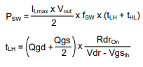
PS: other companies define formulas like this: Pic (left top formula)
https://www.analog.com/media/en/technical-documentation/data-sheets/3957afa.pdf#page=13
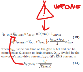
PS: I note, some TI guide uses wrong formula to determine Pdcond. If you use real switching Iswrms or Iswavg current at FET (the maximum RMS inductor currents are approximately equal to the maximum average inductor currents) under full T period, then Dmax correction (multiply with Dmax at powe dissipation) does not need anymore. If you use general inductor rms/avg current under full T period then using of Dmax is right. These two viewpoints are mixed in TI's guides. This is confirmed in MATLAB simulations too.
Formula 9-10:
https://www.ti.com/lit/an/snva168e/snva168e.pdf#page=4
Formula 10 and 14 calculates real RMS current signal form on FET for full T period, so formula 9 and 14 does not correct with using Dmax.
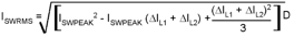
FYI: correct precise formula for rms current on FET under full T period is here: formula 38
https://www.ti.com/lit/ds/symlink/lm3478.pdf?ts=1612941395766#page=25
Please confirm them.
Best regards,
Attila