This thread has been locked.

If you have a related question, please click the "Ask a related question" button in the top right corner. The newly created question will be automatically linked to this question.

LM5146-Q1: Input/Output transience

Part Number: LM5146-Q1
Other Parts Discussed in Thread: LM5146, LM5069

Hi there

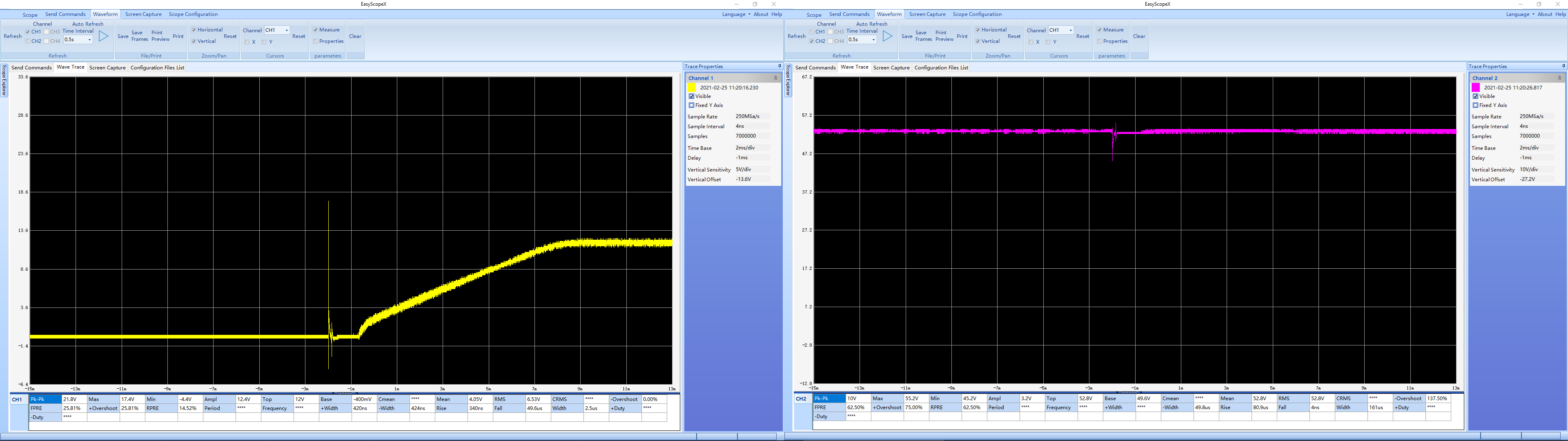
I am facing an issue with the LM5146 buck. I am using it for a 58V to 12V 5A application.


When the input of "58V" is given to the buck through a two pin connector, a huge transience is observed at buck input as well as output. It can be seen in the image attached to this post. The yellow waveform represents buck output and the pink one represents its input.

The input transience ranges from 21.6V to 60.8V and the output transience ranges between -3 to 24.2V.

Kindly help us understand this phenomenon.

  • Hi Abhijeet,

    Are you applying a step voltage to VIN? If so, this may be capacitively coupled across the high-side FET parasitic capacitance and thus transferred to the output. You can try reducing the input dv/dt and make sure the input filter is adequately damped by using an electrolytic cap [= 4 * Cin] and a series damping resistor [= SQRT(Lin_parasitic/Cin)].

    Regards,

    Tim

  • Hi Tim

    I am actually applying a Step input. This phenomenon will occur only once in our system when the board is connected to the battery through a connector, after that the board is always powered on. The issue is during just this one time, the LDO on the 12V line fails sometimes because of this output spike.

    I captured these new waveforms with a series resistor (4 Ohm) before the input power connector.
    The input as well as output spikes appear to be reduced.
    On plugging and unplugging multiple time I did not see a peak of more then 13 or 14V (I discharged the input capacitors before every plugin).

  • Hi Abhijeet,

    Yes, that looks like coupling through the MOSFET and inductor parastic capacitances directly to the output following the step input. This is mostly topology related.

    Here are some steps:

    1. Check if the high-side gate to source voltage is blipping (if so, add a 10k gate-source resistor to mitigate this).
    2. Select a high-side FET with lower Coss (specifically Cds).
    3. Connect an electrolytic input bulk cap on the input to reduce the dv/dt -- or use a hot swap circuit (e.g. LM5069).
    4. Larger Cout helps to absorb the spike.

    Regards,

    Tim

  • Hi Tim 

    Thanks for the suggestions, will try them out tomorrow.

    I was thinking of putting a TVS diode at the output. kindly share your thoughts on this solution?

    I was also discussing about this problem on the EEV forum and there they are suggesting that this has something to do with the impedance between my input, output and buck's gnd. Something like this:

    It seems likely to me because of the huge loop being formed by my input, output as well as the buck's gnd

    Kindly let me know your thoughts on this.

    Regards

    Abhijeet

  • Hi Abhijeet,

    Use a Zener instead of a TVS as it has a more accurate clamp level.

    In terms of PCB layout, as long as you have a solid GND plane on layer 2 connecting the various GND vias, it should be okay. The output caps are a bit far away in your layout, but I doubt that's the main issue related to the VOUT spike when VIN snaps high.

    Best option is if you can reduce the dv/dt of Vin at startup. You can measure the inductor current to confirm the current spike is coming capacitively across the high-side FET.

    Regards,

    Tim