Hello,
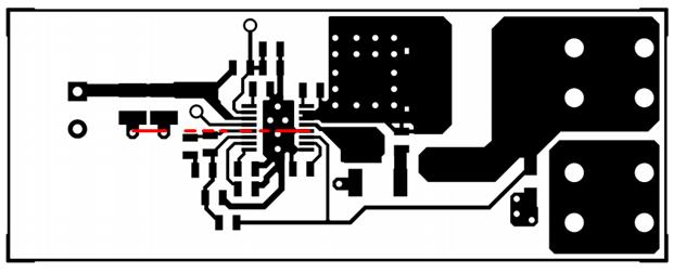
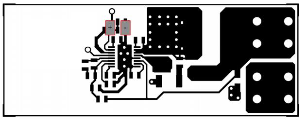
I have read the LM5575 datasheet and the application note "AN-1569 LM5575 Evaluation Board". The datasheet recommends that PGND and AGND are connected through the topside copper area underside the device and the app note shows this connection.
Given that LM5575 has two ground pins, PGND and AGND, I would connect the AGND through a narrow trace to the negative pole of the output filter capacitor rather than to the topside copper area. Doing so, the regulator should be able to get a more accurate measure of the output voltage. In my opinion, the solution stated in the datasheet would lead to a high noise level on the AGND pin because of the ground connection parasitics (resistance and inductance).
I'd like to know the reasoning which underlies the datasheet (and app note) solution.
Can someone help me?
Regards
Gioacchino

-
Ask a related question
What is a related question?A related question is a question created from another question. When the related question is created, it will be automatically linked to the original question.