This thread has been locked.

If you have a related question, please click the "Ask a related question" button in the top right corner. The newly created question will be automatically linked to this question.

TPS54561-Q1: >500mV peak-to-peak switching noise on DCDC's 5V output

Part Number: TPS54561-Q1
Other Parts Discussed in Thread: TPS54561

Hi,

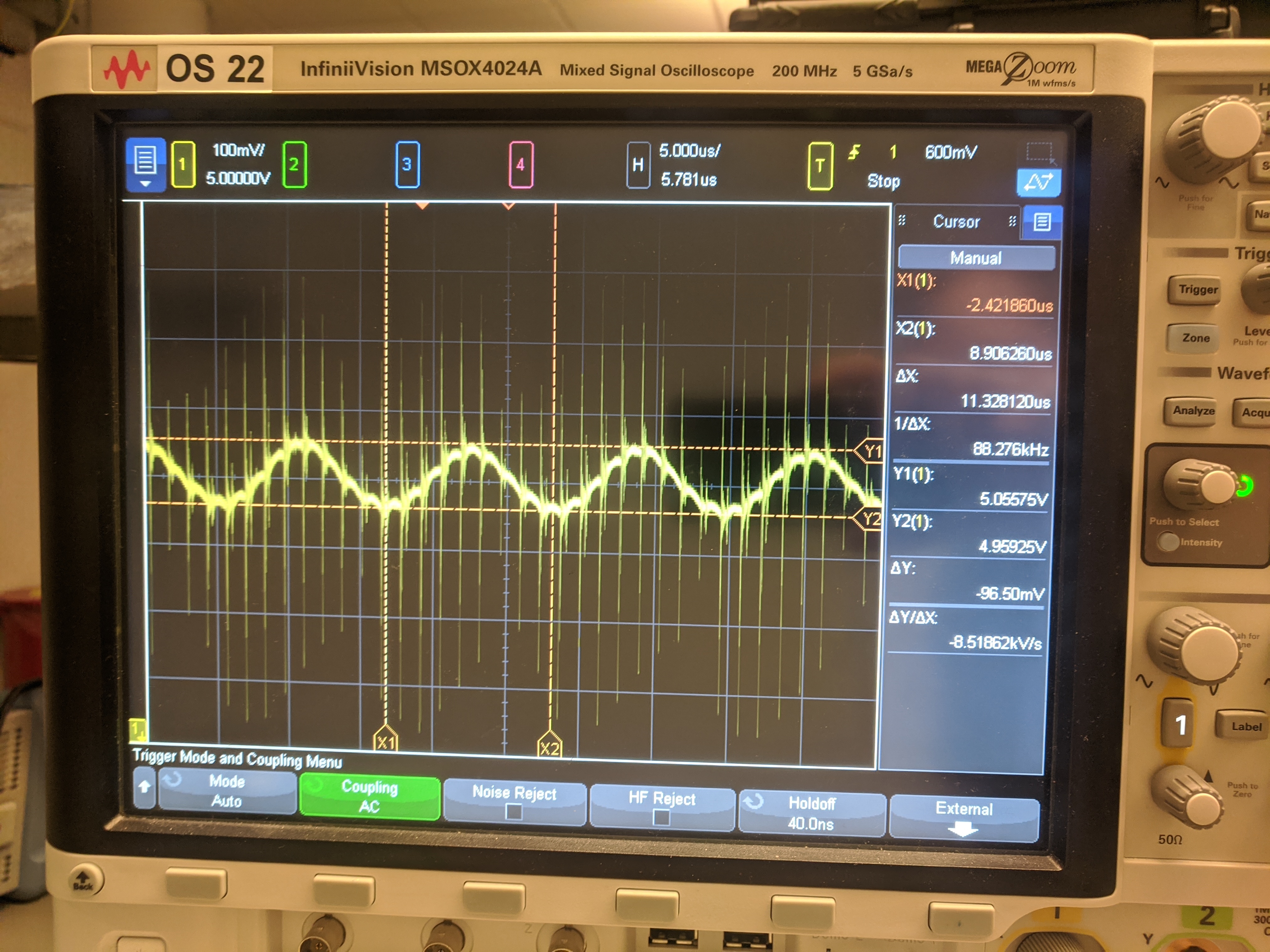
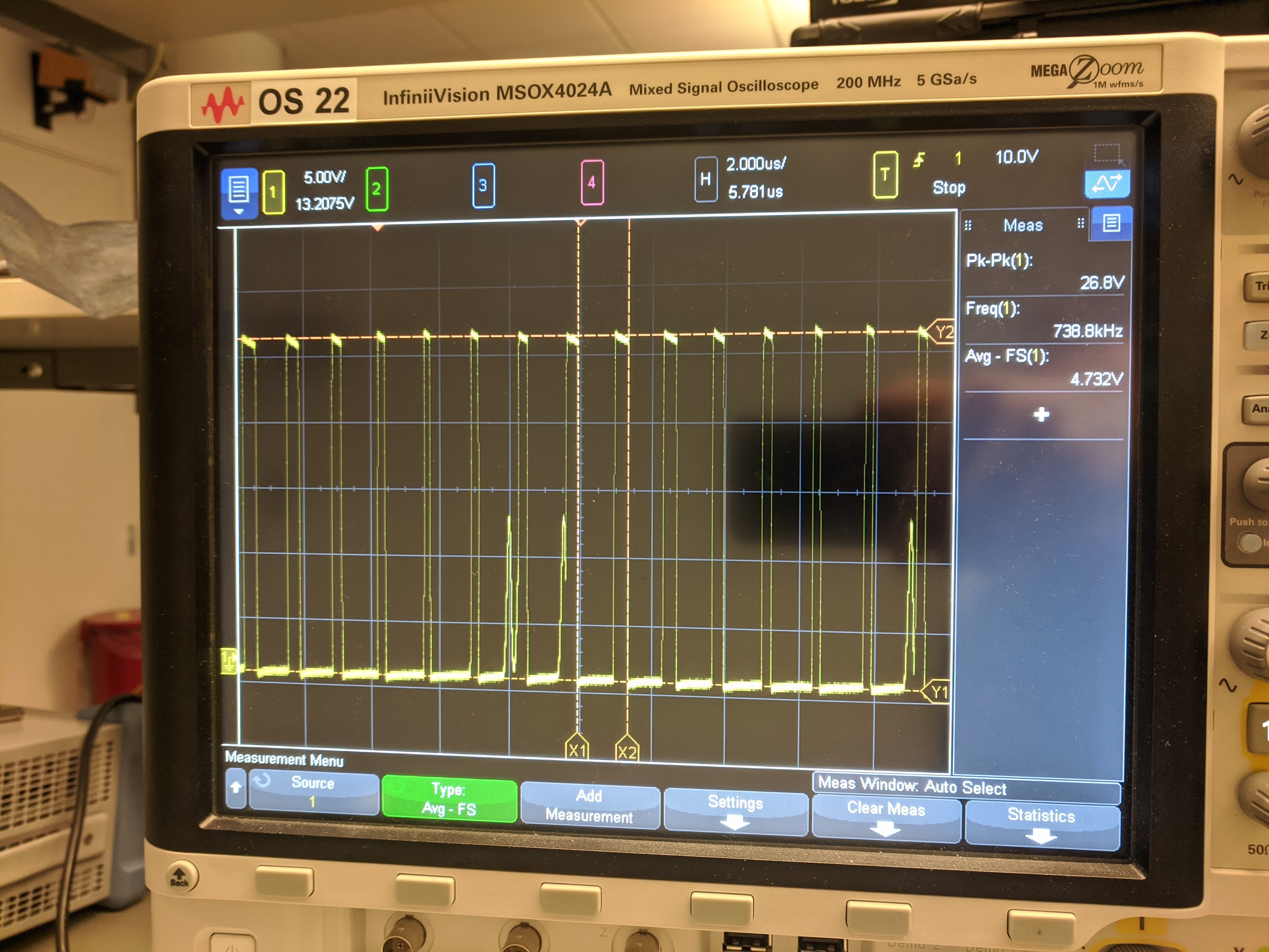
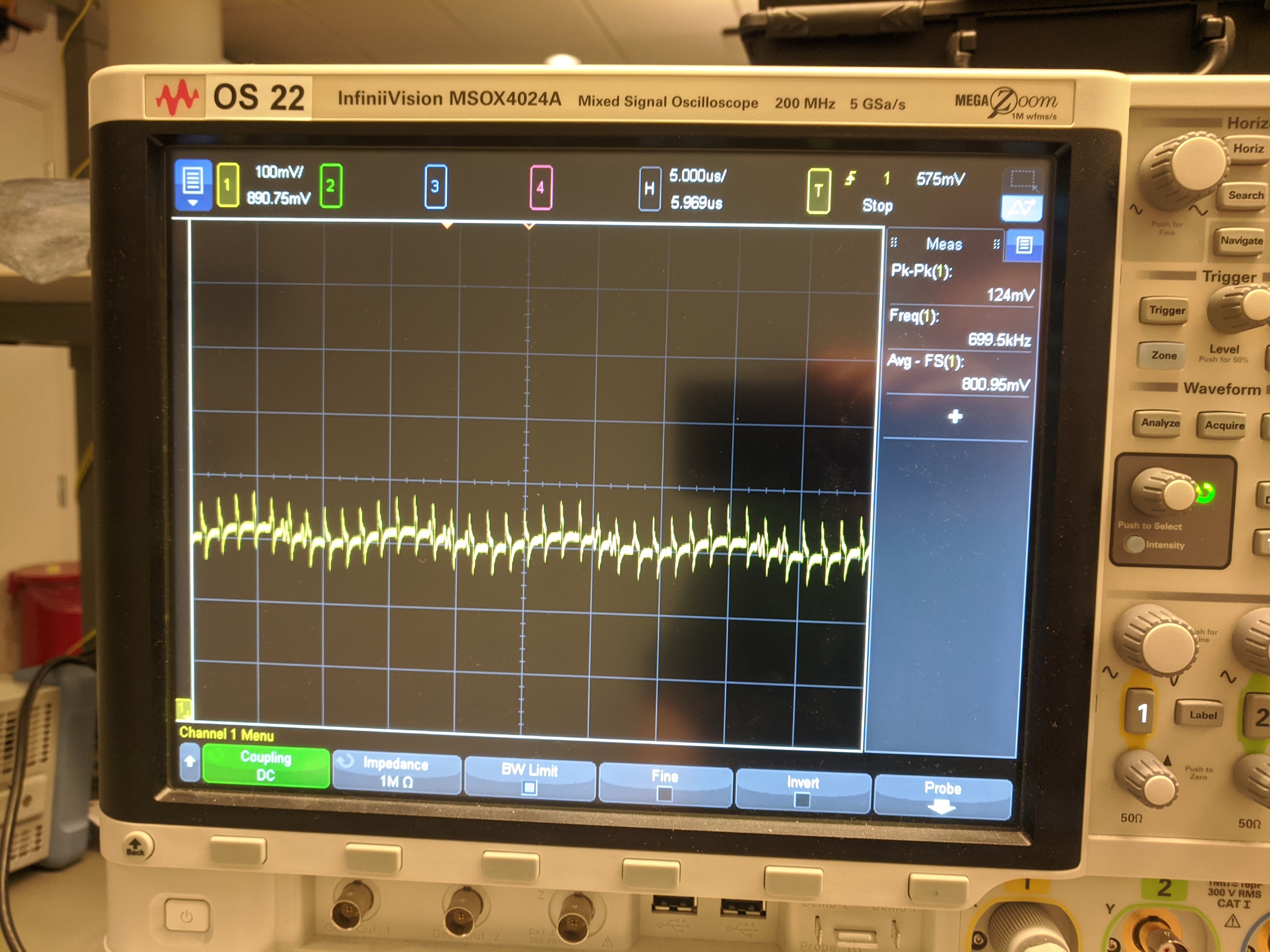
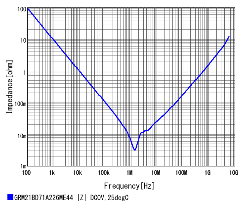
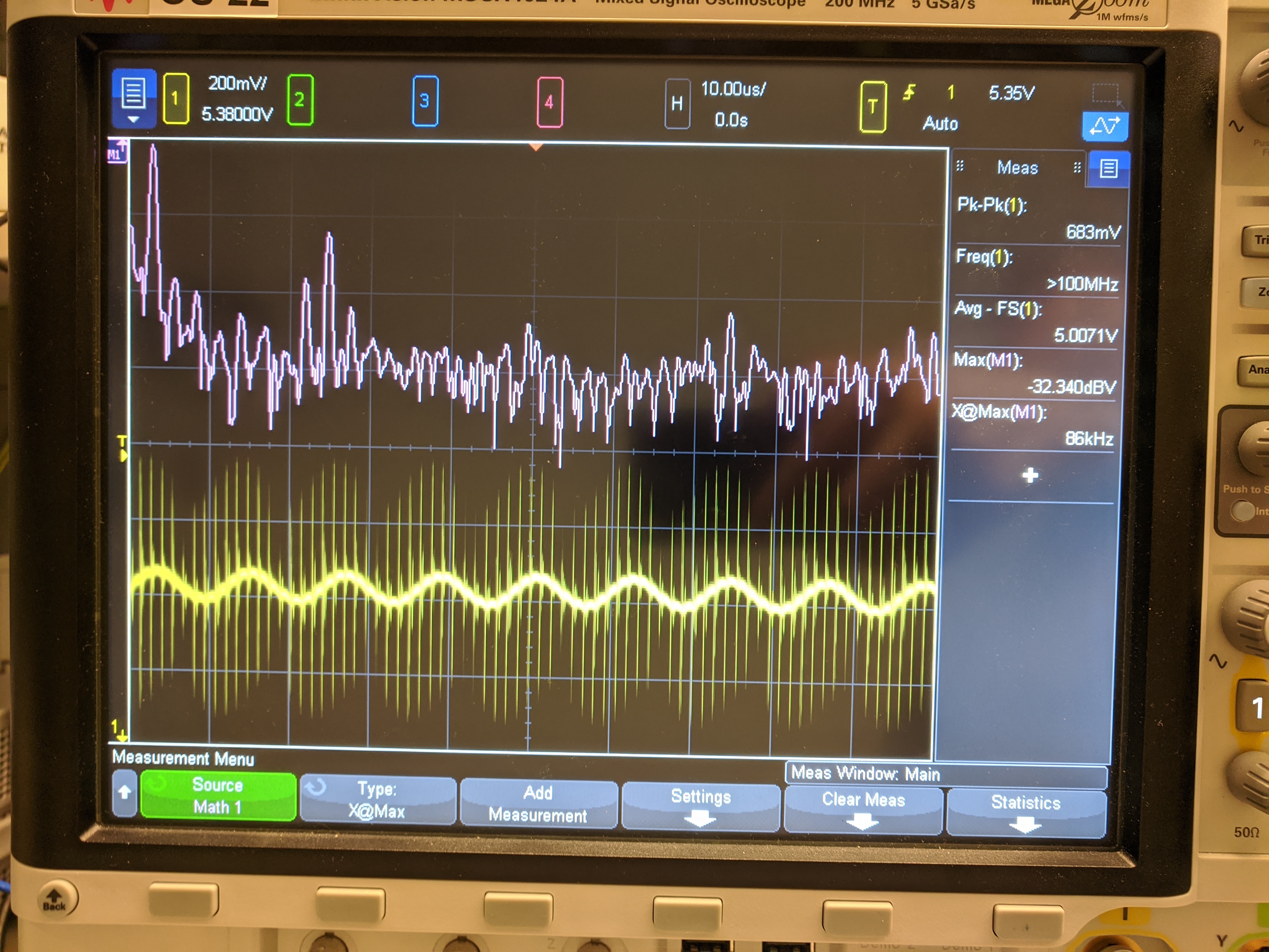
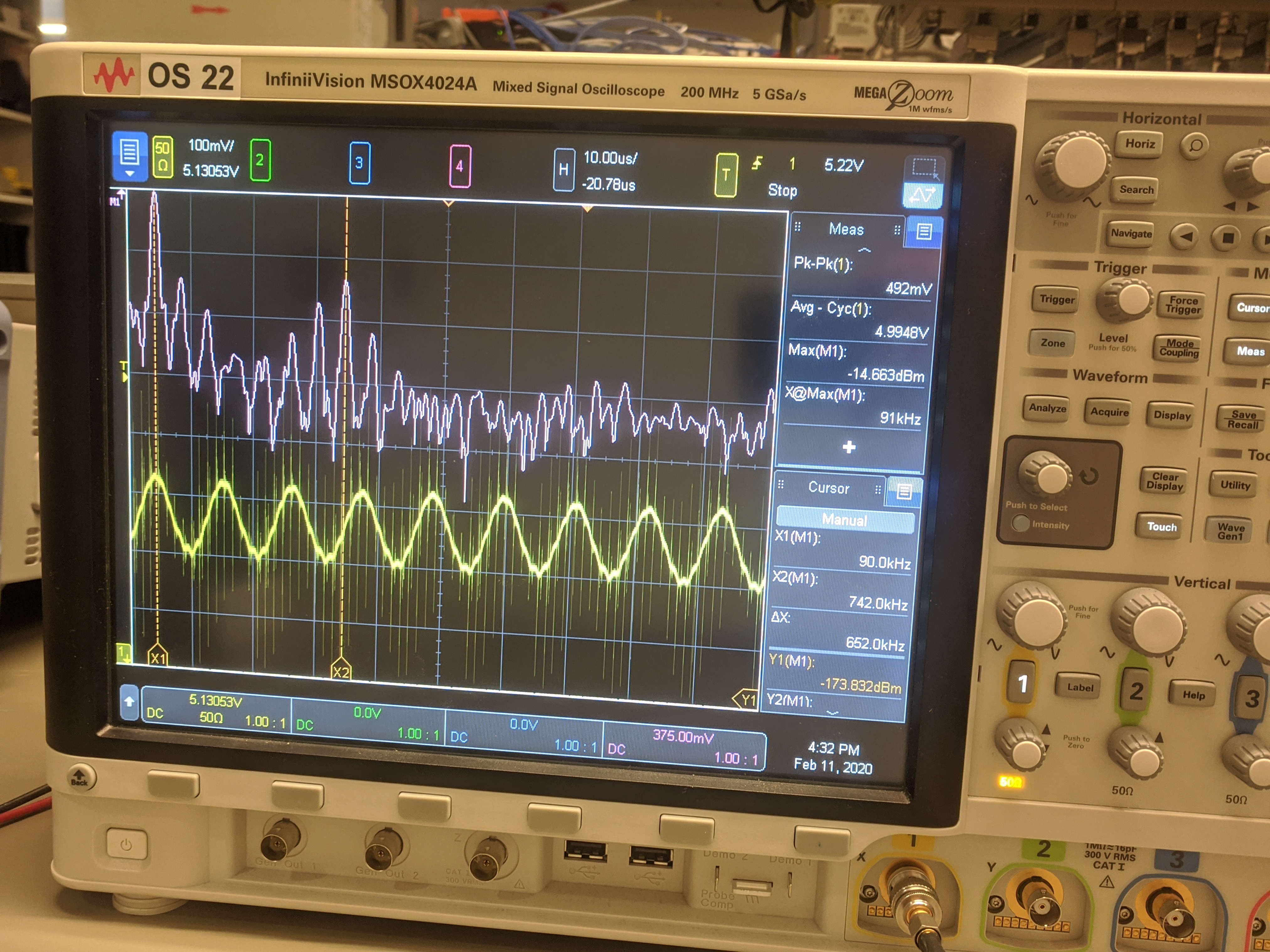
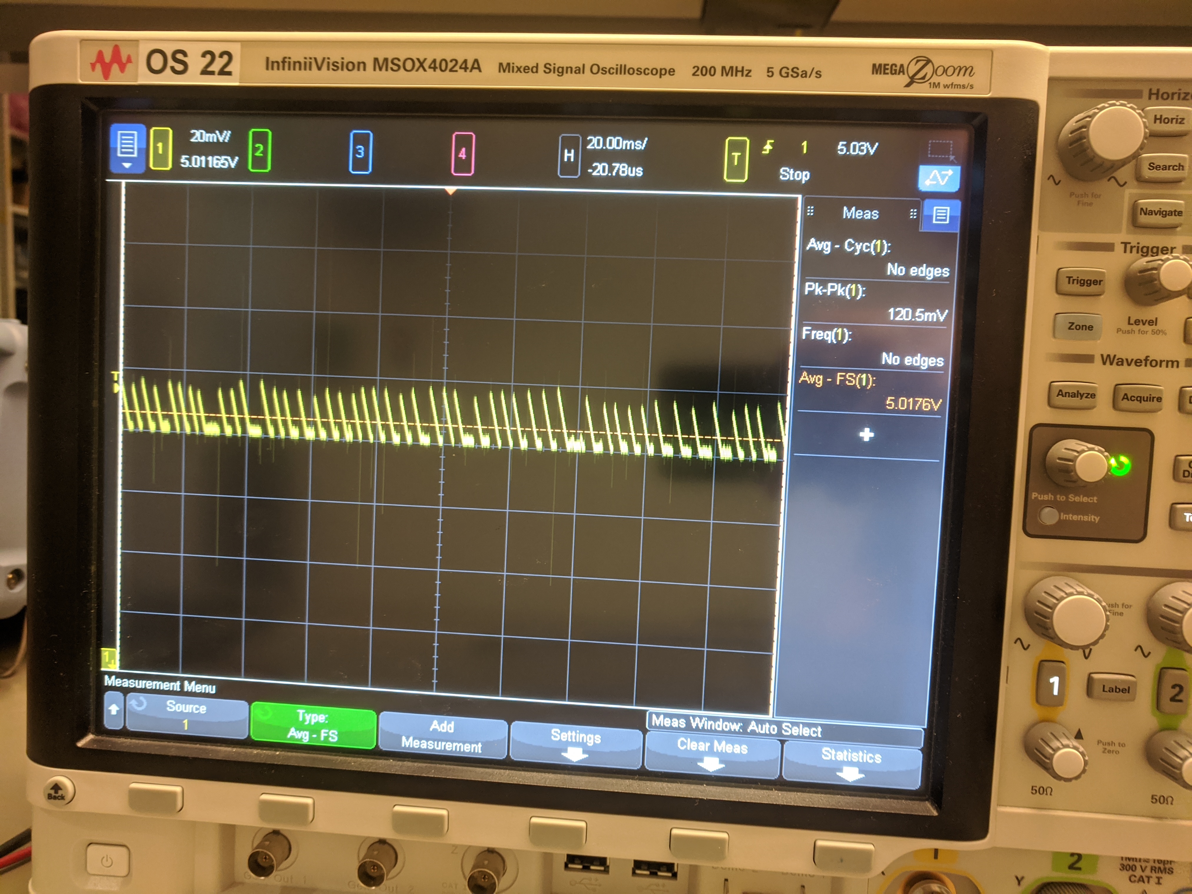
We recently designed a board with the TPS54561 DCDC regulator. The average output voltage is hitting the target of 5V, however we see a switching noise on top of it, with peak-to-peak value of between 500mV and 800mV. This is well above the simulated noise level of 34mV peak-to-peak. This ripple is at the same frequency as the expected switching frequency of the regulator (737 kHz).

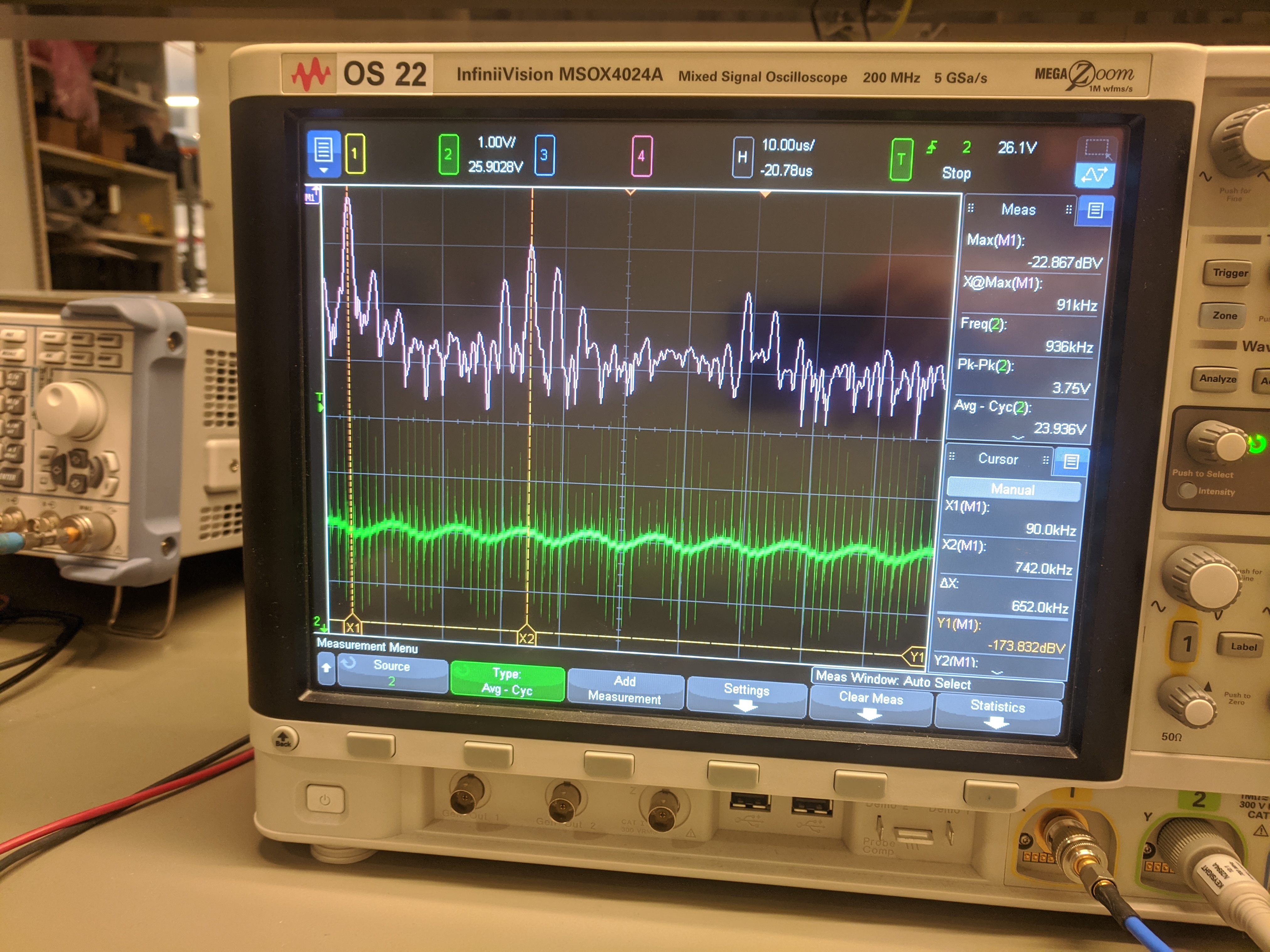
The board is a 10-layer board, with several DCDCs connected in parallel at the TPS's output for further regulation to 3V3 and 1V8. With a power resistor load instead of these DCDCs, the ripple reduces to 400mV peak-to-peak. The regulator typically regulates from a Vin of 24V. We also see this 737kHz switching noise on the input - but then 5V peak-to-peak.

Do you have any suggestion what might be the reason for the noise, and how to correct the circuit to remove it?

So far we see the following possible culprits:
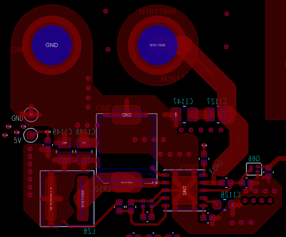
• Lack of ground plane on closest layer underneath TPS IC – next ground plane below chip is on layer 5. There is a ground plane on adjacent layer underneath the larger power connectors (seen as mounting holes in the upper part of the layout snippet).
• Lack of ground vias on DCDC chip's thermal pad

Best regards,

Jonas

Design information

  • Hello Jonas,

    Can you please complete the calculator tool attached here for stability analysis.

    8461.TPS54360-361FAMILY_CALC_TOOL_REVE.xls

    And can you please share the inductor current, SW and VOUT waveform. To accurately measure the VOUT waveform, please have a look at this video.

    https://training.ti.com/power-tips-measuring-vout-ripple-dcdc-converters

    And what type of output cap are you using in your application? What is the ESR of the output caps.

    Best Regards,

    Ankit Gupta

    Application Engineer

  • Hello Ankit,

    Thanks for the answer.

    I've filled in what I know in the excel sheet and so far the suggested values match our design (and the webench output). I will get the circuit designer to have a look at this as well, so that we can fill all fields.

    After seeing the video you linked I understand that the noise I talked about is not ripple, it's the high frequency switching noise.

    I did new measurements with and without limited bandwidth, resulting in a ripple measurement of 100-130 mV.

    Without BW limitation:

    With BW limitation:

    Isn't the high switching noise coupled into my circuit from the DCDC's output anyway, and something we would like to remove? Should we put a high frequency ceramic cap on the output like shown in the video you linked? We also see a 5V peak to peak switching noise on the input, and we have already tried a larger 1 mF electrolyte on this node without much effect, but maybe that cap had a too low frequency spec?

    Here is the SW node, BW limited (without the BW limitation the peak to peak increases to 34V):

    With my layout I don't think I'm able to measure inductor current. In case you would like to see it, here is the feedback node voltage (BW limited) - this comes from a "11.5/(60.4 + 11.5)" voltage divider connected to 5V (should be 800mV):

    The output caps are two 22uF GRM21BD71A226ME44L in parallel. I'm unsure what frequency the ESR should be reported at (it seems there are different ways to do it), but at the resonant point of 1MHz it is 3mOhm. At our switching frequency (at approx. 700kHz) it is 2mOhm. I see some SMPS ESRs are reported at 100kHz - there it is 4mOhm.

    |Z| from Murata simsurfing ():

    R from simsurfing

    Best regards,

    Jonas

  • Hello Jonas,

    Answering your questions here:

    Isn't the high switching noise coupled into my circuit from the DCDC's output anyway, and something we would like to remove? - No, it is just the radiated noise from SW node getting coupled into the loop formed by your probe used for measuring VOUT. If you just keep reducing the size of the loop formed by the probe, you will observe much reduction in coupling with radiated SW noise on your probe. That is why on the video engineer uses a pigtail probe to have a minimum possible loop on the probe.

    Should we put a high-frequency ceramic cap on the output as shown in the video you linked? - Yes, it will help to filter out the high-frequency noise coming from SW to Inductor's capacitive winding and finally to the output.

    We also see a 5V peak to peak switching noise on the input, and we have already tried a larger 1 mF electrolyte on this node without much effect, but maybe that cap had a too low-frequency spec? - But most likely it will be radiated noise only. Try using a pigtail probe across the VIN Cap. Hope this helps!

    Please close this thread if you think your issue is resolved.

    Best Regards,

    Ankit Gupta

    Application Engineer

  • Hello Ankit,

    This was my suspicion too, so I have measured with a semirigid coax soldered onto the DCDC's output copper plane. The measured switching noise was then approximately the same level.

    Maybe there is larger than normal AC ground loop, caused by lack of thermal vias & adjacent ground plane, which radiates the switching noise throughout the circuit?

    Disregarding the switching noise, there is still a ripple that is four times higher than the value from the Webench simulation (132 mV vs 34 mV).  

    Best regards,

    Jonas

  • Hello Jonas,

    What is the ESR of the output caps?

    BR,

    Ankit 

  • Hi Ankit,

    |Z| of GRM21BD71A226ME44L is 3 mOhm at the resonant point. There are two of them n parallel at the output, so it should be closer to 1.5 mOhm, unless they mismatch (it's X7T with 20% tolerance). It is 50% derated at 5V.

    See also graphs of |Z| and R of the cap in my answer from Jan 29, 2020 3:30 PM

    I have added 100 nF caps in parallel at the output as well, and measured just some 100 mV decrease in peak to peak switching noise.

    - Jonas

  • Hello Jonas,

    You mentioned you had ripple on Vout of about 132 mV and now by having 100nF caps at output decreases the peak to peak switching noise by 100mV. Which means the present switching noise 132mV-100mV=32mV. Is my understanding is correct here?

    Best Regards,

    Ankit Gupta

    Application Engineer

  • Hi Ankit,

    Switching noise and ripple are two separate frequency signals. Switching noise is the one at the switching frequency, while the ripple is a sinusoid at a lower frequency (as described in the training video you linked in your first post).

    I don't think the switching noise is something we can disregard, as this is still present when probing with a coax semirigid (and loading with a power resistor in parallel with a 100 nF high frequency MLCC).

    Below is the coax probe measurement with this load. The noise is distinctively two frequency components - the switching frequency at 737 kHz and the sinusoid ripple at about 80 kHz. The switching noise seems to be enveloped at the frequency of the the ripple signal.

  • Hi Jonas,

    Can you provide a photo of coax wire soldered or connected to output capacitor?

    Pls disconnect 5V output to downstream converters if possible. and connect 5V to E-load or resistor load with output current round 1A~1.5A

    If low freq 80KHz ripple still exist, and not see such ripple on Vin, then the control loop maybe not stable as duty cycle was obviously unstable on your above thread. pls use 3pcs 22uF16V--25V ceramic cap  on output only and calculate the COMP pin value again by Circuit Calculator.

    Pls also add 0.1uF 100V cap parallel with C1127 and C1147.

    Pls test output ripple with only input channel connected to Scope, Set Scope input resistor to 50 ohm when test with coax wire.

    B R

    Andy

  • Hi Andy,

    Would be great to hear if you have any input as to what might be the reason for this noise - too high ground impedance, too much space between passives and IC, too high ESR at input, too low resonance frequency on caps? At this point we are thinking we will abandon the current design, and rather copy the TPS54561 EVM as we have tested this now. It's able to supply 5V to the planned load with about 100mV peak-to-peak ripple+noise.

    To answer your questions

    Below is a pic of the coax soldered on the output copper plane.

    My load is purely resistive (7.5 Ohm), no downstream converters are connected. There's 0.2 Ohm between coax wire and the power resistor's leg.

    I don't have any more power resistor's so I can't increase the current (now around 667mA). I have one modification of the original DCDC components at this point: two 2.2uF 100V in parallel at input.

    But still the same output ripple + noise is present. Measurement was improved when changing to 50Ohm probe. Measurement is shown in the second picture below.

    Input measured with same conditions, using oscilloscope probe.

    Output with no load (only the original two 10V 22uF output caps in parallel):

    I added 0.1uF 100V cap (GRM31C5C2A104JA01) in parallel with the input caps, and the result is about the same (still measured with semirigig coax):

    I can't answer all of your questions now:

    • Calculate the COMP pin value again by Circuit Calculator.

    Do you have a link to this circuit calculator?

    • Pls test output ripple with only input channel connected to Scope

    What do you mean with this question?

    Best regards, Jonas

  • Hi Jonas,

    Circuit calculator link as below:

    8461.TPS54360-361FAMILY_CALC_TOOL_REVE.xls

    I mean that test output ripple with only ONE input channel connected to the Scope.

    Pls solder the coax wire to Cout cap terminal, NOT on the load resistor terminal.

    Pls solder coax wire as above, set Scope input resistor to 50 ohm, the ripple value is 2X the value measured by Scope.

    B R

    Andy