This thread has been locked.

If you have a related question, please click the "Ask a related question" button in the top right corner. The newly created question will be automatically linked to this question.

UCC21710-Q1: Current sense monitoring through shunt, with a SiC mosfet with kelvin source connection.

Part Number: UCC21710-Q1
Other Parts Discussed in Thread: OPA365, , UCC21710

Hi,

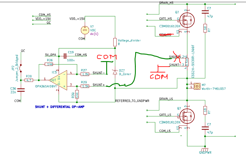
I'm developing a buck converter where I'm using a leg with two C3M SiC mosfet from Cree with kelvin source connections, with a DC bus voltage of 800V (I attached the printed pdf from kicad). The load is an inductor connected from the switching node of the leg to the power ground GNDPWR. I'd like to place a shunt resistor in series to the high-side switch to monitor the current and manage the overcurrent protection. For this purpose I chose a 0.5mOhm shunt and set the short circuit threshold at 150A, having a correspondent voltage of 75mV across the shunt. Then I use the OPA365 as difference amplifier, supplied at 0-5V, to amplify this voltage to reach 0.7V required to the OC pin of UCC21710-Q1 to detect the fault. The problem arises here since the OPA output is referred to its negative supply voltage (0V) that is the power ground power, but its output should go to the OC pin, referred to the COM of the UCC21710-Q1 that include the kelvin source loop.
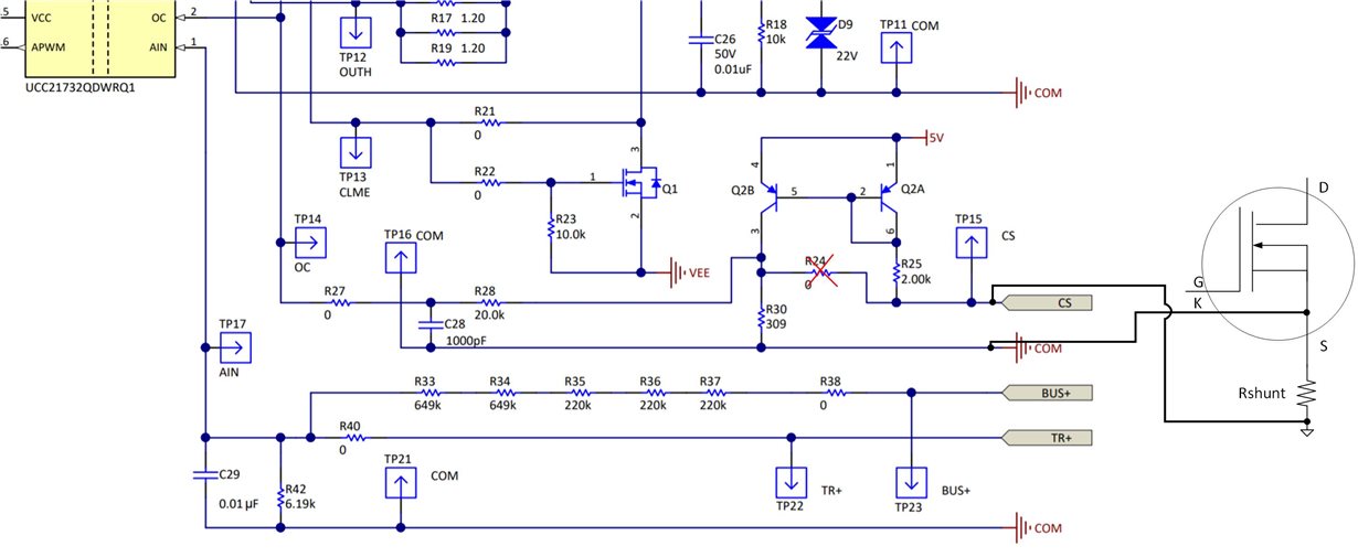
Same problem with the current monitoring through the isolated amplifier SI8920AC, where the isolated reference (pin 4) has been connected to the negative lead of the shunt to reject the common-mode voltage (as suggested in its datasheet), but its 5V isolated supply voltage (pin 1) is obtained from a DC-DC still referred to the power ground. Of course I need an isolated current sensing decoupling the COM-kelvin loop to the GNDPWR for the OC detection and avoiding high common-mode with the SI8920AC.
How can I manage the kelvin connection to use the shunt resistor and separating all my isolation ground loops? I was wondering about connecting the load between the switching node and the DC bus voltage, and placing the shunt in series with the low side source pin, but still I should connect together the low side kelvin pin and the PWRGND, loosing the isolation.

Thank you in advance.

Stefano8103.Printing Print Schematic.pdf

  • Stefano,

    Thank you for your question, and I appreciate that you have already posted the schematic.

    You are correct, the problem with using that OPA365 is the reference to ground and not highside IGBT emitter voltage, is there a particular reason to measure on highside? I see that the high power consumption means we could not increase the shunt any more, so an amplifier is required to do signal conditioning. easiest option, is to use the OPA365 on lowside and move the shunt resistor there. Or you can share VDD/VEE rail of the highs-side driver with OPA and keep the shunt resistor on the highside.

    6292489 said:
    I was wondering about connecting the load between the switching node and the DC bus voltage, and placing the shunt in series with the low side source pin, but still I should connect together the low side kelvin pin and the PWRGND, loosing the isolation.

    Could you please clarify what you are saying by this, I am not so sure about what you are meaning. I think placing the shunt in series with the low-side is the simplest and best way.

    Best

    dimitri

  • Hi Dimitri and thank you for your quick reply,

    the main reason to measure on the high-side is to have a fast short circuit detection. Now the load is going to be connected between the connectors M2 and M3, so it charges up through the high-side and discharges through the low side, therefore if a high current or shot-through condition occurs, the origin is in the high-side.
    Sharing the VDD/VEE of the drive is actually a good idea (I used the MCP1799T to regulate the 15V to a 5V), I totally forgot about that supply voltages. Still, I have up to 800V of common mode at the inputs of the OPA365 and SI8920 and I don't know if some trouble can come up.

    dimitri james said:

    Could you please clarify what you are saying by this, I am not so sure about what you are meaning. I think placing the shunt in series with the low-side is the simplest and best way.

    My other idea is to connect the load between the connector M1 and M2 and then connecting the shunt on the low side having a symmetric circuit with respect to the current case. 
    I'm quite new in these kinds of power circuits and I don't know what is the difference between having a load referred to ground or to my 800V.

    Stefano

  • Stefano,

    Thanks for explaining, i understand why you need to do the high-side current sense!. As far as referenced to ground or Emitter/source of IGBT/Mosfet, this high-side sensing is not uncommon using the floating highside supplies to power the amplifier

    To reiterate, the extra amplification is not required if you increase the value of shunt resistor to something on the order of mOhm rather than 1/10ths of mOhm, with some additional benefits. Of course, there is the cost of more power consumption thru the shunt resistor.

    I think the below configuration could work. Shunt(-) Pin connect to COM, Kelvin connection and COM are used as inputs to your amplifier you use for signal gain. This uses Kelvin connection for its specific purpose of getting more accurate voltage measurements fromsource.If your amplifier VDD need is much lower than VDD of your gate driver, then you can use something like a zener to regulate it down.

    This concept is shown in this Reference design for 3phase motor drive to do the phase current sensing (although, in that reference design, its using an Isolated AMC1300B amplifier since the gate driver used there doesn't have the same features as UCC21710, the concept is the similar.

    The topology of how the current sensing is done starts on page 17. Its essentially not much different from your need for high-side amplification of shunt resistor differential voltage. Also shows how the supply for that ampplifer is generated (Zener for VDD and highside COM/IGBT emitter)

    6292489 said:
    I'm quite new in these kinds of power circuits and I don't know what is the difference between having a load referred to ground or to my 800V.

    Understood! We have a great resource explaining the differences between high-side and low-side shunt current sensing

    Please let me know if you have any more questions on this!

    Best

    Dimitri

  • Dimitri,

    I've read the files, a very interesting and useful application, thank you. However, I think the problem here is my fourth terminal that introduces an intrinsic limitation in my circuit: looking at page 18 where the current sensing is explained, the reference voltage is given by the zener from the +15V (referenced to DC- pin shared with the low side ground reference!) of the driver and referenced to node U_G1 (the switching node of the leg). In this case, it works, but in mine I have my 15V of the driver referred to a different node with respect to the ground of the low side. If I use the solution proposed in the application I would have the anode of the zener connected to the switching node that sweeps from 0 to 800V (referred to PWRGND) and the cathode connected to a 15V referred to COM (i try to attach a draft schematic of this idea to be more clear). The conflict between the two power loops and the high common mode is unavoidable I think.

    Remaining with the idea of the high-side sensing, I think at this point it is necessary an isolated op-amp for the OC protection too, in order to have the isolated side powered up with a 5V generated through the system voltage divider + zener and referred to the switching node, and the output side connected to a 5V referred to the kelvin source node (COM). 

    I really hope to have understood well my circuit without introducing more problems than the necessary ones and not to mess up your mind more than before...

  • Stefano,

    What youve shown is a little different than what I am suggesting. but similar.

    Keep in Mind, COM for the highside can be considered as a high-side ground, and your isolated voltage source will generate the 15V highside supply referenced to COM, so really the zener is only going to have to regulate 15V down to 5V, not 800V to 5V. If that were the case we should see smoke.

    I am not sure if my last image was uploaded, i can't see it.

    This is what i was suggesting:

    Best

    Dimitri

  • Dimitri,

    The picture has been uploaded correctly, but I do not understand your corrections: first I would specify that the COM node is the same as COM_HS in my picture (I forgot to specify it, but I think you understood my intentions), then in my opinion when you connect the SHUNT- node with the COM you have all the common mode back to the dc-dc converter that generates the 15V for the drivers.
    One solution that came up to me is to use an isolated dc-dc converter from an external voltage from a power supply I use to power up the board (ON_SWITCH label, +12V) and obtain a 5V isolated and referred to the SHUNT- node. Then I use this voltage to power up the isolated part of the SI8920AC, that amplifies the differential signal of the shunt (0.075V) by 16.2. At its output, I regulate that voltage through a voltage divider to obtain the 0.7V needed for the OC pin (the output of the SI8920AC is differential referred to its COM, so I only take the positive one for the OC) and I supply the output part of the SI8920 through the zener system from the 15V of the driver (so I have this side referred to COM). Then I can use another SI8920AC as before to sense the shunt voltage and bring it to the microcontroller reference.

    It should work on paper, don't know if is too complicated as a solution.

  • Stefano,

    I undertand that COM/COM_HS are same node.

    6292489 said:
    then in my opinion when you connect the SHUNT- node with the COM you have all the common mode back to the dc-dc converter that generates the 15V for the drivers.

    What is your concern here? Are you referring to the potential ~75mV common mode shift caused by the shunt resistor?

    Could you share about how you are generating your highside bias supplies?

    Your suggested idea is OK, but that is a lot of effort just to connect COM directly to the emitter of the IGBT rather than after this. In your schematic above, your isolated amp's only purpose would be to do a very small level shift. There is no need for this. It could work but its very very overcomplicated solution to a simpler problem.

    If you look at the implementation of shunt resistor, the shunt is typically connected in the way I've specifed, and com is always connected to the tail of that resistor, since OC pin references to COM. There should not be any problem for you to follow this way, just inserting your OPA block.

    best

    dimitri

  • Dimitri,

    dimitri james said:

    What is your concern here? Are you referring to the potential ~75mV common mode shift caused by the shunt resistor?


    The switching node (REF_SHUNT) switches between approximately 0 and 800V every time the HS turns on and LS turns off and vice versa, so this is the common mode voltage I refer here. Eventually, I sense the voltage difference across a shunt that swings along the full rail.
    I post below the rest of my schematic. The first image is the high side gate driver with its supply voltages, the second image is the half bridge with the shunt.

    I'm sorry if I insist on this story, but I really want to understand well the situation I'm facing. That schematic reported in the datasheet uses a 3 terminal IGBT/MOSFET, so the COM coincides with the switching node in the case I have a half bridge. But having a kelvin source, the COM is referred to this, and the switching node is in another ground loop.


  • Stefano,

    Sorry for my misunderstanding. My previous suggestion to use Kelvin source to measure , it was misguided, i was thinking this was best solution based on understanding of power devices without a kelvin source connection. Apologies for my confusion on that topic!

    You are right, Kelvin source must connect to COM.

    Therefore, SHUNT+ is also at COM voltage, and SHUNT(-) will be below COM.

    Taking a look at our own EVM board design for COM, is it possible that you could use the bipolar current mirroring circuit ? This will push the voltage up to be referenced to COM. Have you seen this EVM before? A previous question which was answered by my colleague was answered this
    You could base your circuit then, then you wouldn't to have a 5V supply referenced to SHUNT-, you could reference it to COM by using Zener clamp or IC if you prefer.

    https://www.ti.com/lit/ug/sluubx2b/sluubx2b.pdf#page=9

    Best

    Dimitri

  • Dimitri,

    that's brightened my day! I have already read this EVM board design a couple of months ago, but I was not able to retrieve much information about the current sensing part, and I was surprised that this is explained well in the EVM you post here... I just realized that my document was a version updated last May 2019 while this one is referred to June 2020. In my old version, the chapter 1.3.6 explaining the current sensing is very poor compared to the June 2020 one (I post the 2019 version if you are curious to check).

    Thank you and have a nice day!

    UCC217XX_eval_board.pdf

  • Stefano,

    I am glad we got this figured out. Have a good weekend!

    Best

    Dimitri