This thread has been locked.

If you have a related question, please click the "Ask a related question" button in the top right corner. The newly created question will be automatically linked to this question.

LM25141-Q1: LM25141-Q1 questions

Part Number: LM25141-Q1

Hi,

I'm trying to configure LM25141-Q1  for a design

VIN=12V

VOUT=5V/10A

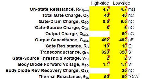
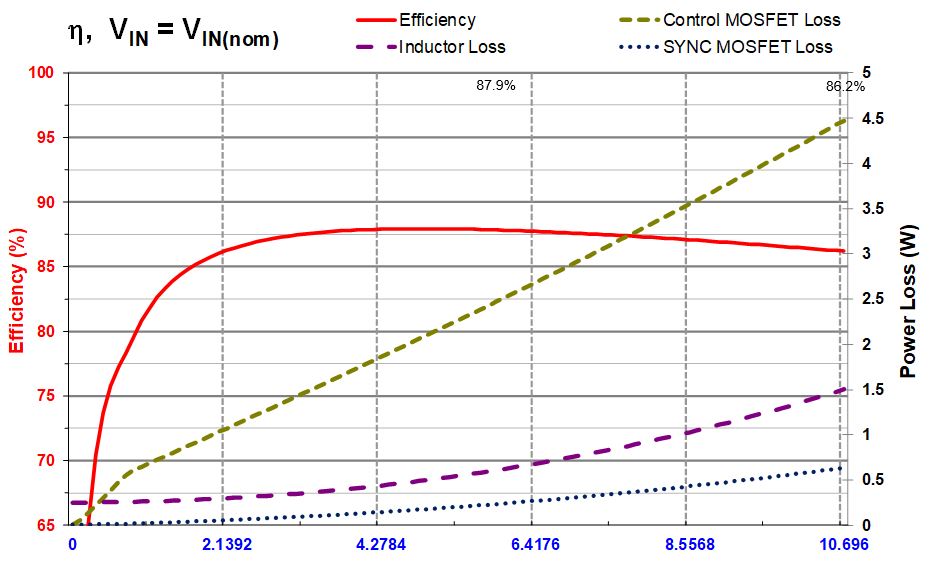
1) For the reference design -https://www.ti.com/lit/df/tidrsr2/tidrsr2.pdf?ts=1591205504535

May i know the purpose of  R16 and R19 . Is it for noise filtering also please let me know why R19 is zero ohms.

2) For VCCX can i pull it to the regulated 5V output and do i require 2.2uF at VCCx ( i couldn't find recommendation for the same in datasheet) but it seems mentioned in LM25141-Q1 Quickstart Tool - revA2.xlsm design tool from TI

3) For DEMB pin i understand there is dual function i.e. to enable diode emulation and as synchronization input to synchronize the internal oscillator to an external clock.

If i want to use diode emulation as well as external synchronization , Is it possible? how shall i connect it? ( or may be I'm thinking wrong).Please suggest.

Thanks,

Stephen

  • Hello

    Yes, you can use the attached design as a reference for a 5Vout design.  And yes it is good to use the calculator tool to assist with 

    the design.  Keep in mind that the design you attached is somewhat generic, so some components may be optional or just place holders.

    The exact configuration will depend on what is needed in you specific design.

    With this device you can also use the built in feed-back divider for 5Vout, if you wish.  The data sheet shows how to do

    this.

    1. R16 along with the associated capacitor is for noise filtering.  If your were to use the internal feed-back divider, then the VOUT pin

    is used to sense the output voltage.  In that case R19 would be replaced with a 10-50 ohm resistor for measuring the loop stability.

    In the case of the example design you attached, R19 is more of a place holder.

    2. Yes, you can connect VCCX to the 5Vout of the regulator.  In this case the 2.2uF would be optional.

    3. When using the DEMB input for a synchronizing signal the device will be in FPWM mode; I don't think there

    is any way around that.

    Thank you

  • Thank you very much for the reply.

    With the excel design tool also i have a few more doubts,

    1) Row 87 is specified as  RG ,  which i assume is RHO/RLO i.e resistor connected to HO and LO pin. Is that right? 

    I have kept RHO and RLO as 10R,  then my efficiency takes a major down step and goes to ~88% ( from ~ 93% if i had kept it at 1.4R ). 

    My MOSFET approximate parameters are as below , and corresponding power loss figures are also shown


    You can see the control MOSFET dissipation is on higher side with 10R gate resistance. Is it advisable to keep Gate resistance in 1R range here. Or any other factors like slew rate control (EMI aspects ) come into picture there

    Im seeing for https://www.ti.com/lit/df/tidryp0/tidryp0.pdf?ts=1591205502376 a 10R is used

    but for https://www.ti.com/lit/df/tidrsr2/tidrsr2.pdf?ts=1591205504535 lower values are used. 

    So what parameters exactly decide this resistance value.

    Thanks

    Regards

    Stephen


  • Hello

    I believe that RG in the spreadsheet is the sum of the internal FET resistance and the external resistance.

    So you would find the gate resistance for your FET and put that in there, along with any value of external 

    resistance you are using.  

    Of course all of the other values for the specific FET you are using would also need to be input to the calc.

    I think that the procedure you are using is correct.  Adjust the values of the components and see the effect.

    If 10 ohms gives too much loss, then a smaller resistance (or 0) is indicated.

    Larger values will slow down the gate drive, helping to improve EMI.  At the same time larger values

    reduce you efficiency. 

    So that is the biggest trade off.

    Thanks

  • hello

    I will close this post due to inactivity.

    Thanks