This thread has been locked.

If you have a related question, please click the "Ask a related question" button in the top right corner. The newly created question will be automatically linked to this question.

UCC27211: questions when used in boost

Part Number: UCC27211

Hi, 

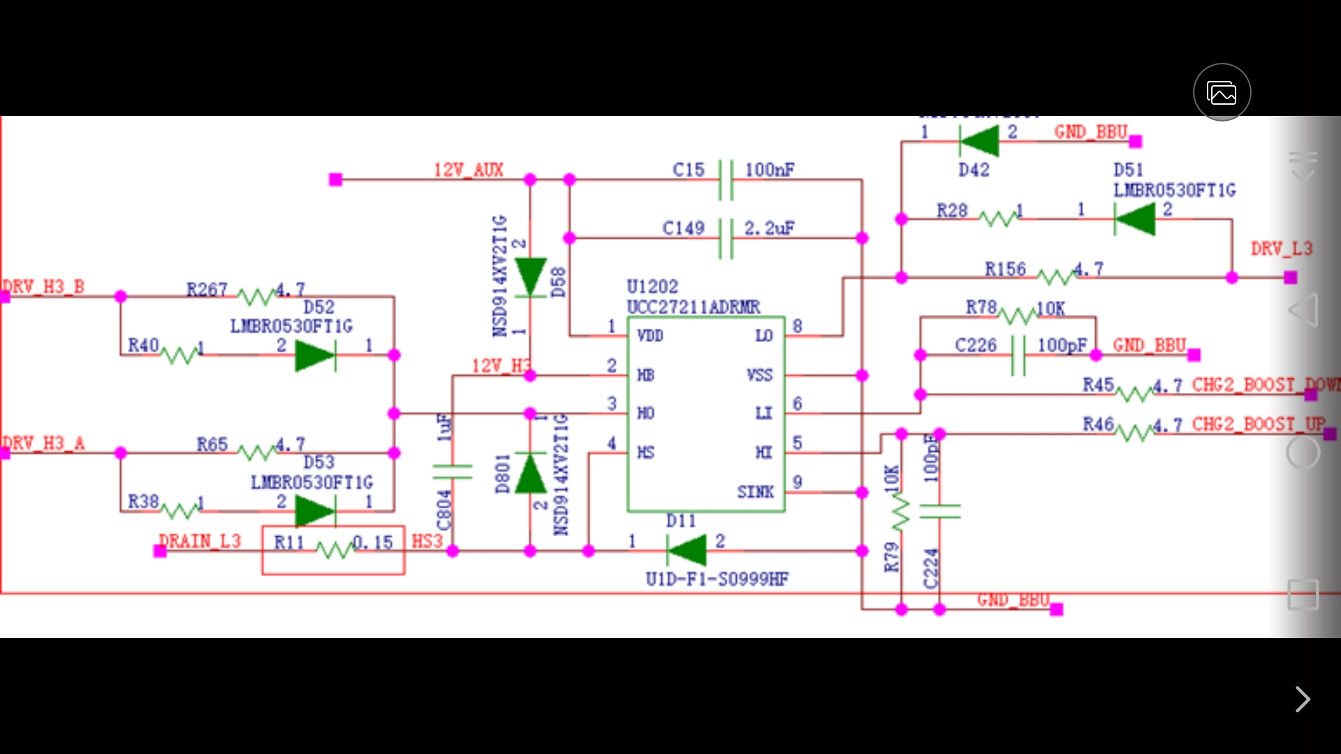
UCC27211 is used in a boost topology. 

pin 8 : driver for LS  MOS  

pin3 : driver for HS MOS 

Drain_L3 : connect to SW 

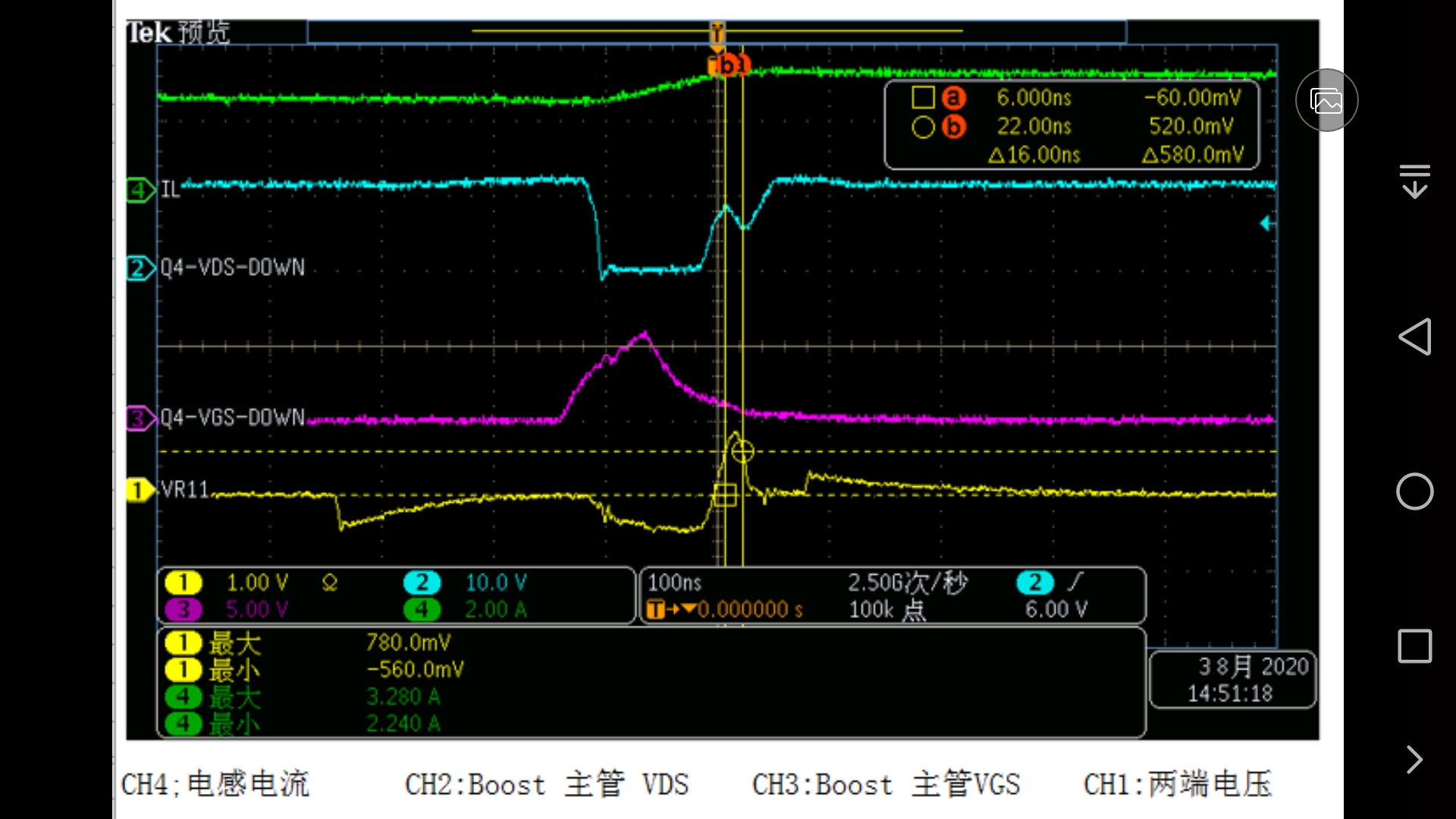
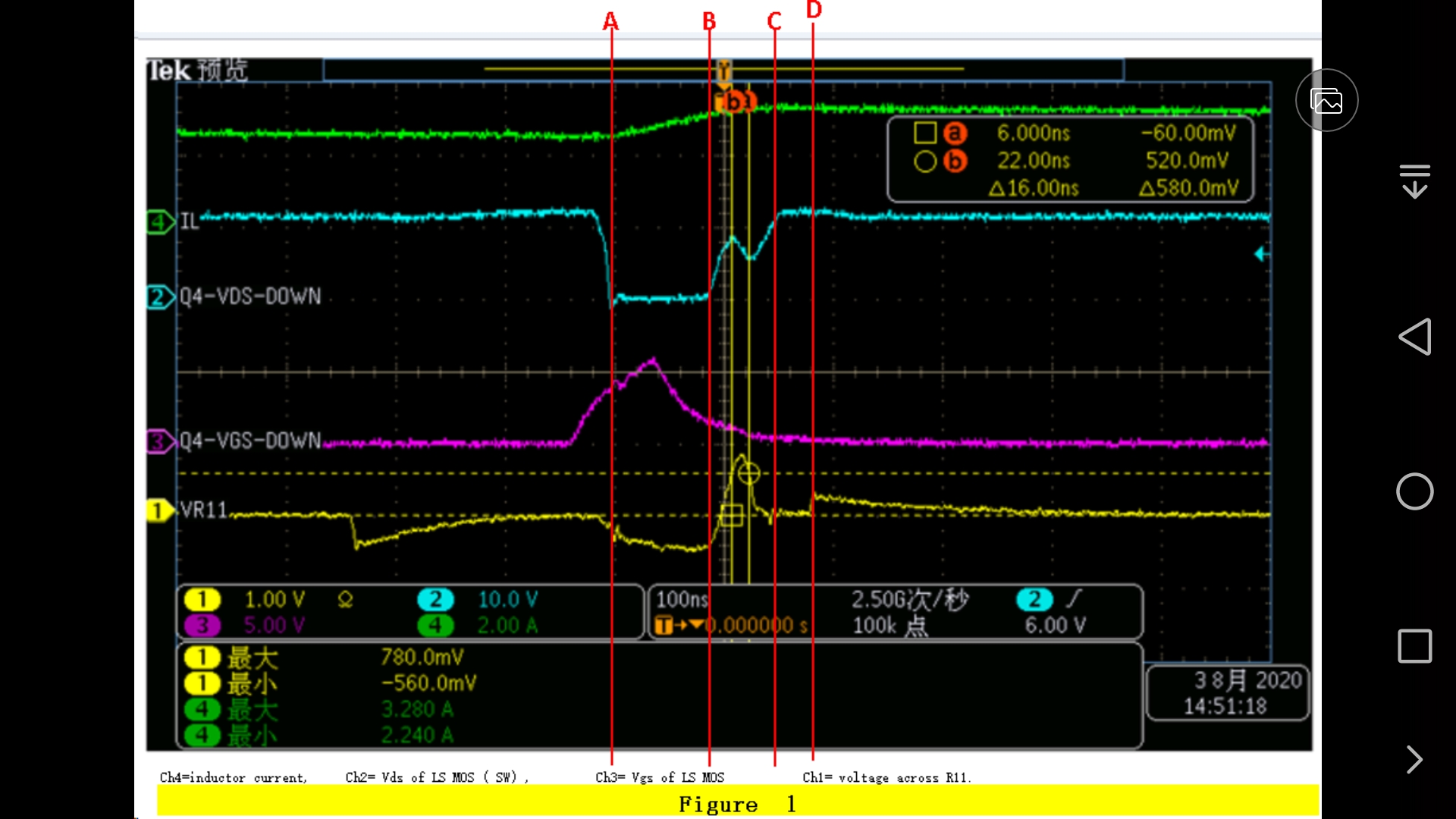
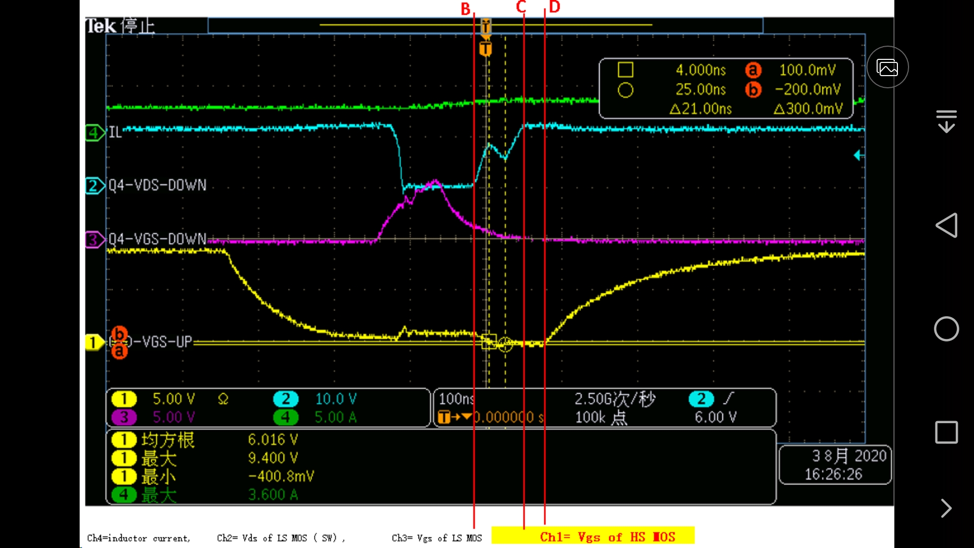
Ch4=inductor current, Ch2= Vds of LS MOS ( SW) , Ch3= Vgs of LS MOS Ch1= voltage across R11. 

From the waveform, when LS MOS is turned off, there is 5.5A current from DRAIN_L3 to IC. 

#1, what's the reason for the current ? 

#2, does the current has effect on IC itself? 

Thanks. 

BRs

Given 

  • Hello Given,

    I did not see a scope waveform plot along with the post information. I do see the schematic, but not the waveforms.

    It sounds like the concern is there may be high current from drain L3 to IC HS pin. Can you confirm if this current was determined by the voltage across R11?

    Without seeing the waveform it is hard to comment in detail. But the voltage measurement across R11 will be subject to noise so the probing would have to be very close to the resistor terminals. Also there is likely high common mode voltage on both resistor terminals so a differential probe would have to be used.

    Can you include the scope plot referenced in the channel descriptions?

    Regards,

  • Hi Richard,

    Thanks for your reply.

    sorry for missing the waveform. Please kindly see below. thanks.

    BRs

    Given


  • Hello Given,

    There are two possible causes for the voltage across R11 in the scope plots you show. The boot cap is charged thru the path of the VDD cap thru the boot diode and charging the boot cap thru the switch node when the switch node switches to ground. Since there is the resistor between the boot cap connection to HS and the drain of the low side Mosfet, the boot cap charging current is thru R11.

    Also the HO gate drive current is from the HB cap thru the driver device and the return current path is the HS pin. The HO gate drive current will be thru R11 when turning on or off the HS MOSFET VGS.

    The voltages across R11 I think are either the boot cap charging current, which is into the boot cap, or the HO gate drive current which is expected out of the IC HO pin.

    Regards,

  • Hi Richard,

    Thanks for your reply.

    Still need more detailed explain.

    1. R11 is measured using differential probe, so there should be no common mode noise.

    2. customer's main concern in B-C in below.

     in A-B, Ch2 ( Vds of LS MOS) is low, voltage across R11 is caused by boot cap charging current

    in B-C, 

    a. Ch2 begin rising, current through R11 is reversed, it should not be boot charging current.

    b. HO is low ( Ch1) ( see below waveform), it should not be HO gate current, so I suspect it's boostrap diode reverse current in IC itself. Is it reasonable?

    3. in D, HO rise, current through R11 is HO gate current.

    Thanks.

    BRs

    Given

  • Hello Given,

    Thank you for pointing out the customer concern. After inspection, I think your assumption is correct. Just before "B" the voltage across R11 corresponds with boot cap charging current, and it does not decline to near zero. When the HS rises the boot diode will need to turn off and the R11 voltage reversal is likely the boot diode reverse recovery current.

    Many differential probes are still subject to common mode noise, unless you have a very expensive one. I would still confirm if there is some signal pickup in the probe, since this is happening at a fairly fast voltage rise time. You can do that by just having both probe connections to the HS node and see if there is any induced voltage on the differential measurement.

    Regards,