This thread has been locked.

If you have a related question, please click the "Ask a related question" button in the top right corner. The newly created question will be automatically linked to this question.

UCD90120A: UCD90120A

Part Number: UCD90120A
Hi TI team,
In one of my project I am using the TI power controller IC UCD90120ARGC for the Zynq 7000 SoC power on sequencing.
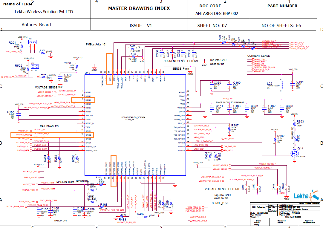
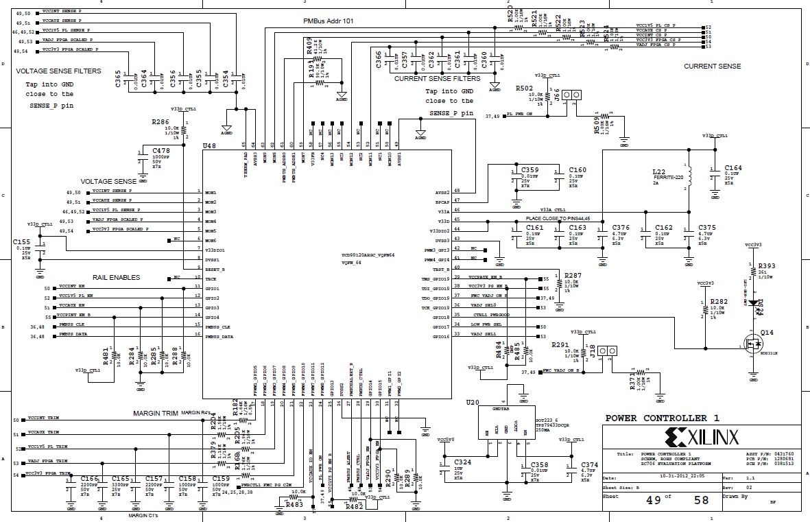
All the power enabling, controlling, monitoring are same as ZC706 development kit except there is changes in the Enable pins at GPIO2 (attached snap shot of the same),
for GPIO2 (power on sequence is same for VCCP1V2_EN_B as VCC1V5_PL_EN) disconnected MON3, MON9 and FPWM3_GPIO7 signals. I have imported ZC706 .xml file and made changes as shown in the Fusion digital power designer(I have removed voltage, trim/margin and current for the GPIO 2 based signals).
I request you to review it once, also request you to generate the file in Fusion Digital Power designer based on our requirement.
Waiting for your valuable reply soon.
  • Hello

     I am not sure understand what you want to achieve here? Do you plan to use GPIO2 anywhere in the system?

    if not, you can just click the Pin 63 MON9 from the GUI, click the remove PIn 63 MON9 from the top of the pop-up windows.

    Click " Write-to-Hardware" followed by "Store RAM to Flash" to make the change permanently.

    After these changes, you will have dummy rail #3.

    Please watch the training video to understand how to use the GUI.

    https://training.ti.com/fusion-digital-power-designer

    Regards

    Yihe

  • Hi Yihe,

    Thank you for your response.

    I use the GPIO2 to enable the 1.2V regulator LMZ31704RVQ.

    The power on sequence followed in the ZC706 and Our card is same. sequence for the VCCP1V2_EN_B  and VCCP1V5_EN_B  remains the same for the GPIO2 pin. Does rest of the power rail dependent on VCCP1V2 monitor, trim, signals?

    Can I use same binary file of ZC706 to program my card.

    Also may I know whether power controller can be programmed multiple times? This is mainly needed because if the programed binary doesn't work at first shot as per our requirement?

    Waiting for your valuable reply.

    Regards,

    Rekha.

  • Hello

    I am still little confused about what you want to change here.

    The ZC706 is not developed by TI. For any application related to the ZC706, you may contact the vendor to get help.

    From your schematics, MON3, MON9 and FPWM3_GPIO7 are not used any more. it is ok to remove from the configuration file

    So your rail#3 is still a valid rail which includes the GPIO signal only after removing all pins.  

    you can program the devices multiples time.

    Regards

    Yihe

  • test.7z


    Hi Yihe,

    Thank you for your response.

    Now I am  facing the problem with respect to VADJ_FPGA_EN rail. Power controller is not asserting the signal high for GPIO14 and its always low, this enable signal is connected to the LMZ31506RUQ regulator. Vadj sel 0 and sel 1 is able to give 00 for the selection of the frequency for the LMZ regulator. (attached code i have used and programmed). I request you to review once. Also i request you to create the one more code which has got only enable signals (as per power on sequnecing requirement)  and not monitoring and PWM signals.

    Power controller able to assert enable signal for rest of the regulator except this. I am stuck in between the board bring up. Please suggest me what to be done next.

    Waiting for your valuable reply.

    Regards,

    Rekha.

  • Hello

    The GPIO14 is the ENABLE for the rail#4(VADJ). it has many sequencing on dependencies.

    In order to have GPIO14 HIGH, the following conditions must be met:

    1. GPIO12 ->HIGH, GPIO20->LOW

    2. PMBUS_CTRL shall be HIGH

    3. The voltages of Rail 1/2/3/4 must be over POWER_GOOD threshold. For rail#3, since it is a rail without monitoring pin, as long as GPIO 2 is HIGH, it is considered over POWER_GOOD threshold.

    Please check above in your system.

    Regards

    Yihe