This thread has been locked.

If you have a related question, please click the "Ask a related question" button in the top right corner. The newly created question will be automatically linked to this question.

UCC27211 : ucc27211

Part Number: UCC27211
Other Parts Discussed in Thread: UCC27282

Hello.

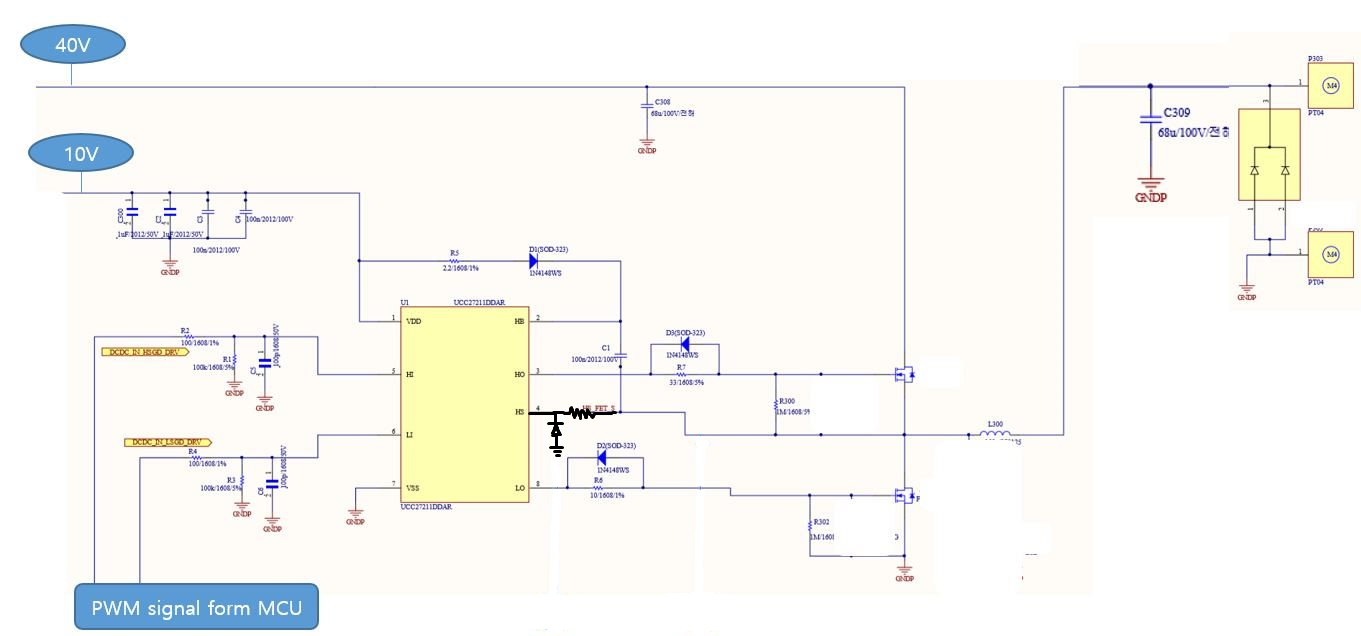
I'm using the UCC27211 gate driver for my project. 

  -Project description :  DcDc  Buck converter, PWM duty 50 ~ 90 %,  frequency 40khz 

  I need to know how to protect HS pin in the below my sch . 

  Can you let me know which one is better for using resistor?  [A or B]  And how many ohms of resistance do you usually use?

  • Can you see the picture below?

  • Hello Do Seoung,

    I will be happy to answer your question, but the picture of the schematic did not show in the last message. You can try inserting a file, or picture in the next message.

    Regards,

  • Hi Richard Herring 

    Here is my schematic .  It was something problem with uploading. 

  • Hi Do Seoung,

    Thanks for reaching out and thanks for the schematic!

    You will want to place the resistor in location A, so that the bootstrap capacitor is still directly referenced to the switching node.  This is to make sure you have sufficient V_GS on the high-side FET.

    A resistor value you can start with can be similar to your gate resistors, around 10 Ohms.  Also, note that when you add a resistor on the HS pin, you will have increased resistance on the turn-off path of the high-side FET (therefore increasing the switch-off time), but having the turn-off diode on the HO gate helps.

    One more thing to consider (if you are having large negative voltage spikes on your switching node), is to put a clamping diode from the HS pin to GND, along with the resistor (as shown below).

    I hope this helps and answers your question!  If so, please press the green button, otherwise feel free to follow up!

    Thanks,

    Aaron Grgurich

  • Hi Aaron Grgurich 

    Thanks for your support. But I don't see your picture .

    When I am using a diode and resistor in the my circuit by your recommendation , is it necessary to consider the output side load capacity and FET's switching time?

    Thanks. 

  • Hi Do Seoung,

    Sorry for the image problem, I fixed it above.

    Regardless of the of the additional components, you should consider output loads, switching times, etc. to see how your system will react to the load and how efficient it will be.

    I hope this answered your question; if so, please press the green button, otherwise feel free to follow up again!

    Thanks,

    Aaron Grgurich

  • Hello 

    Thanks for your kindly support. 

    I still have questions.
    Because I want to get minimize issue when I'm using this device for our product. 

    So I need to more detail technical support if possible. 

    1. Need to more detailed technical reason for using diodes and resistors your recommend position. 

       because the datasheet does not contain this recommend .

    2. recommend resistor value spectrum on my sch ( Current HS FET  resistor value is 33 ohm) 

    3. If I switch to UCC27282, is there any part to change in my circuit? (Including the diode and resistor you suggested.)

    thanks 

  • Hi Do Seoung,

    You are welcome!


    Regarding your questions:

    1)  I only suggested the resistor or resistor-diode combination, assuming you had large negative voltages spikes on your switching node that was damaging the part.  Otherwise, the additional circuitry is not needed assuming your circuit stays within the recommended operating conditions in Section 7.3 of the UCC27211 datasheet.  So, if your switching node voltages stay within the specifications below, the additional circuit is not suggested.

    The technical reason is that excessively large negative voltage spikes on the switching node (HS pin) can damage the part.  The resistor on the HS pin allows for some voltage to be dropped across it, therefore less voltage is seen at the pin; but this comes at a cost of limiting the current in the turn-off loop.  The diode works by shorting the HS pin to ground when the switching node falls below ~ -0.5V (a diode drop).  The resistor is still included with the diode to limit the in-rush current into the diode, so it does not burn up.


    2)  Sorry, I do not understand what you are asking here...  If you are asking about what gate resistor value to use, please keep in mind that the gate resistor value affects the FET turn-on speed, power losses, and etc. If the gate resistor is too big, the FET cannot turn-on fast enough which will then affect the switching frequency range.  I think a good starting point is somewhere between 0-10 ohm, depending on the gate charge of your FET's (because this will dictate how much charge is needed to turn on and off the FET.  If able, bench-top testing of your system will be a good start.

    3)  Yes, and for your current schematic, I overlooked the external bootstrap diode you have.  The external bootstrap diode is not needed for both parts (UCC27211 and UCC27282), because they both have internal bootstrap diode (Please refer to their respective datasheets).

    Also, if you were to use the UCC27282 instead, you would have to consider the extra feature of the ENABLE pin, which must be pulled high in order to enable the driver (again, is specified in the data sheet).

    My final comment is to again say that the HS pin does not need the complication of adding the protection circuit if you system will not have abnormal levels of negative voltage spikes (these specifications of how long and how large the spikes can be, are again, specified by the datasheets.)

    I hope this answered your questions!  If so, please press the green button.


    Thanks,

    Aaron Grgurich