This thread has been locked.

If you have a related question, please click the "Ask a related question" button in the top right corner. The newly created question will be automatically linked to this question.

LM5163: Inverting buck fail to CCM, and >1Vpp output voltage ripple

Part Number: LM5163

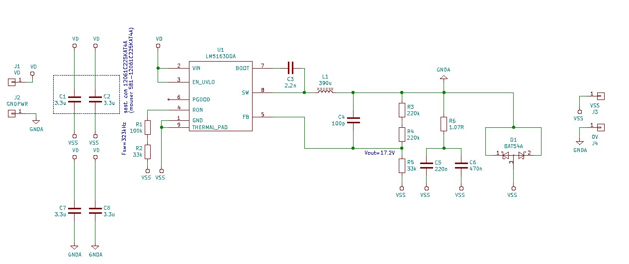
I'm testing a small batch of boards with LM5163 as voltage inverting buck regulator; these are the design specifications: 

Vout=-17V

Vin(min)=36V (ie:18V+17Vout)

Vin(nom)=65V (ie:48V+17Vout)

Max output current= 150mA (70mA nominal with derating due to added safety margin and inverting configuration)

Switching frequency=320kHz

Actual input voltage is +48V and output voltage is -17V @60mA load current.

My concern is the output voltage with a superimposed ripple of 2Vpk-pk in the 8-10kHz frequency range. I think the controller is failing to enter CCM, or something is eating up too much phase margin leading to control loop instability. Also the inductor (Bourns SRR1260-391K from Mouser) is generating some audible "hissing" noise. 

Where am I wrong?

I've read some topics about this controller in this forum, mainly around "type 3" configuration details; is LM5163 supposed to work properly in "type 2" ripple feedback circuit?

This is Webench design:

This is the actual circuit:

  • Hi Eugenio,

    Could you please send over a screen shot of the superimposed ripple on the output voltage, as well as some images of the SW to (-Vout) voltage waveforms.

    If you could send over layout images that would be helpful too.

    The LM5163 should be able to work with type 2 ripple injection, but if your design is unstable then you may need type 3.

    Before attempting Type 3, you may be able to increase phase margin by increasing the output capacitance. Try selecting a 22uF ceramic capacitor with a voltage rating of 35V or greater to account for de-rating. Let me know if this results in any performance improvements.

    Please expect delayed responses due to the Thanksgiving holiday, I will get back to you early next week.

    Thanks,

    Harrison Overturf

  • Hi Harrison.

    This is the board layout (two layers pcb):

    In the following scope screenshot I've acquired Vsw (ch1) and the output ripple (ch2):

    As you suggested I've tried the solution of increasing the output capacitance, but this actually made things worse.

    Then I've read the "AN-1481 Controlling Output Ripple and Achieving ESR Independence in Constant On-Time (COT) Regulator Designs" document (well written document, with a nice intuitive approach), and tried the Type-3 feedback topology.

    This solved the issue! Clean and stable switching behavior (ch1, red), with ~100mV output ripple (ch2, green), at the requested frequency: 

    Adding 47uF electrolytic capacitor lowers the output ripple and does not upset the regulation:

    Now it seems fine; is there any other pitfall I can step into?

    Cheers, 

    Eugenio.

  • Hi Eugenio,

    Thank you for sharing your board layout and screenshots, I am glad to hear that you were able to get this working by following along the app. note above!

     Your layout looks fine, it seems that you just needed to inject some more in phase voltage ripple to the FB pin.

    Be sure to test your design across load currents and input voltages to ensure that the design is truly stable. If you notice any other irregulates feel free to post a new thread so that people with similar issues can search for your question. 

    Regards,

    Harrison Overturf