This thread has been locked.

If you have a related question, please click the "Ask a related question" button in the top right corner. The newly created question will be automatically linked to this question.

LM5160-Q1: Simulation result is quite different from the measured

Part Number: LM5160-Q1

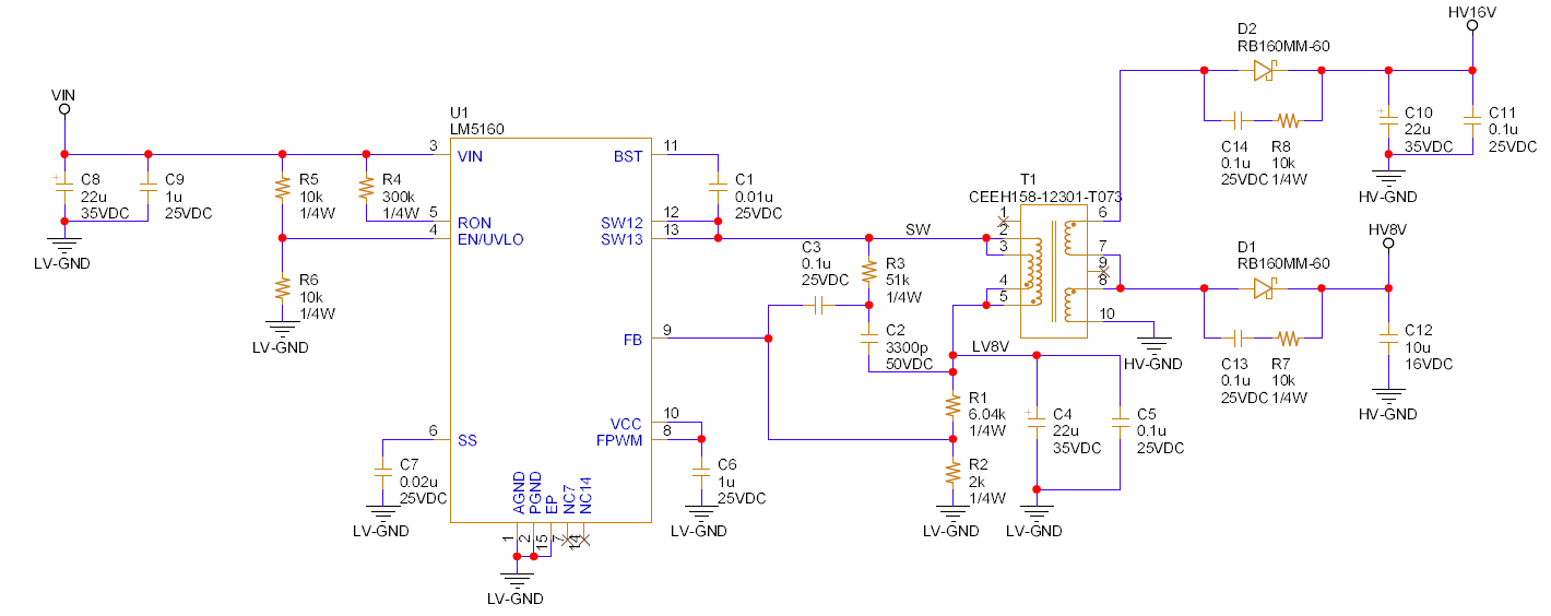
Hello, I have use LM5160-Q1 to make an isolated flybuck converter. The circuit is shown below.

The simulation result looks good. It can control the output voltage to its target value and the process looks nice.

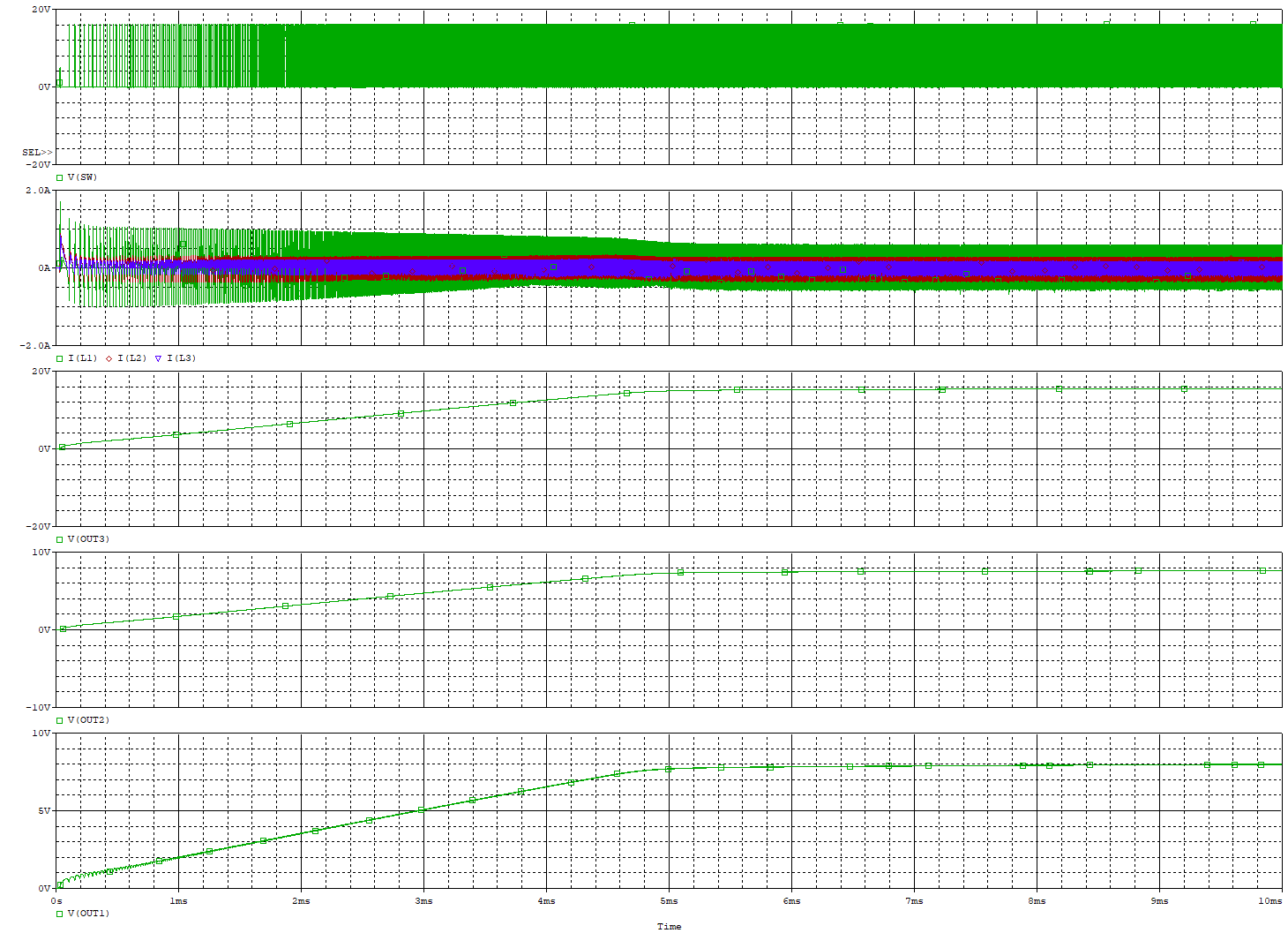
As you can see, V(OUT1) is 8VDC, V(OUT2) is 8VDC and V(OUT3) is 16VDC. The current in the transformer is far beyond 2A.

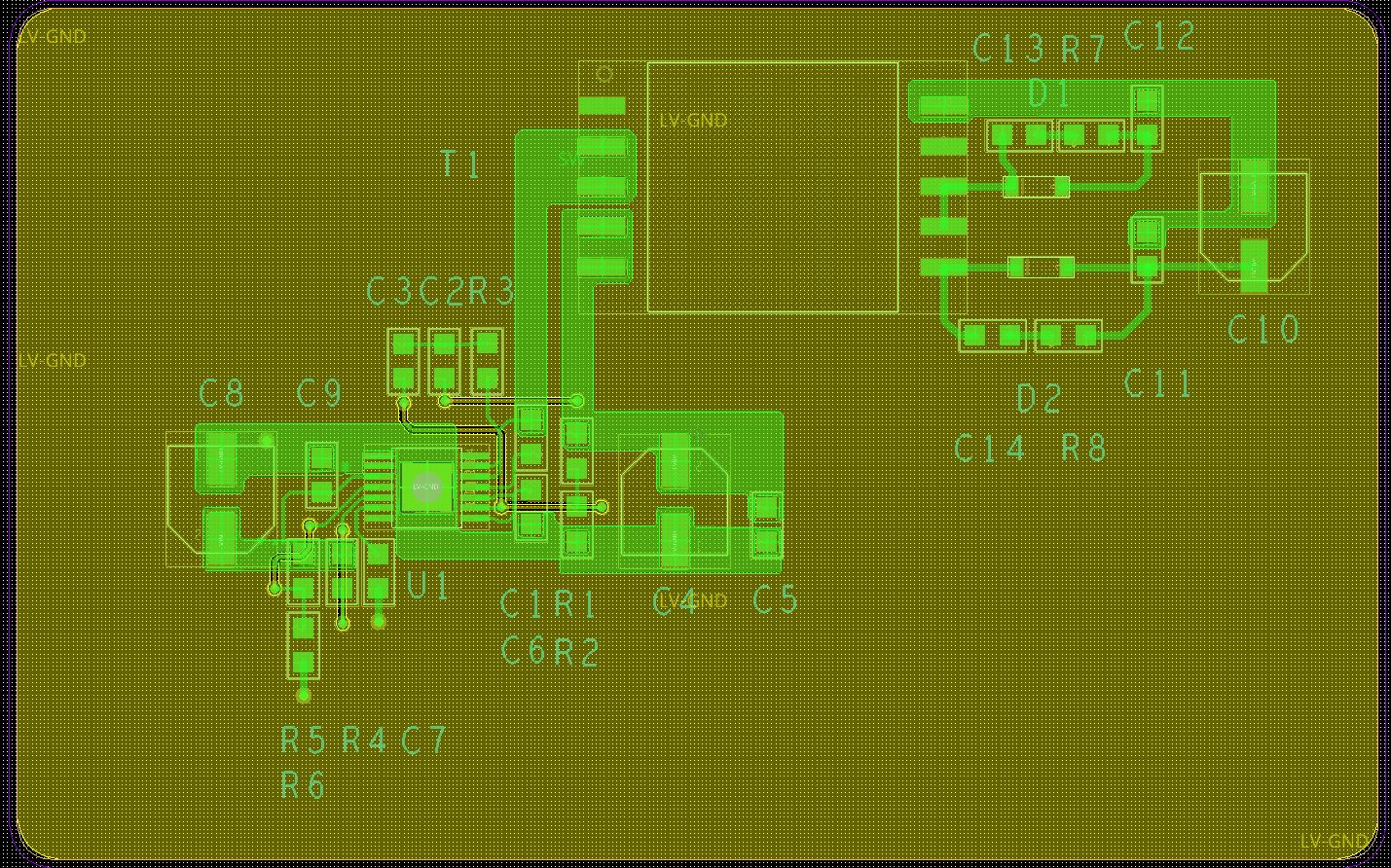
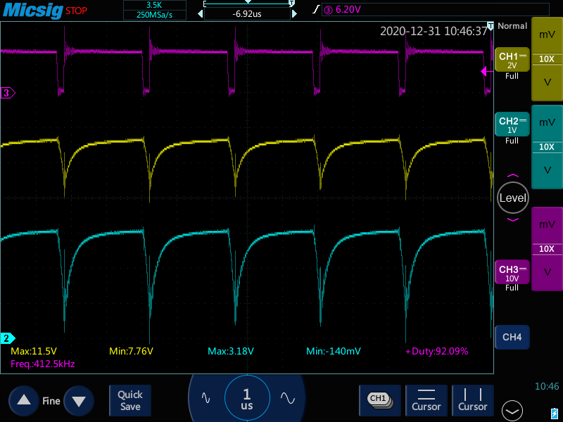
When I measure the related waveforms on the pcb, although the output voltage gets its target value, they look quit different.

Here is the zoomed simulation waveform when the circuit starts.

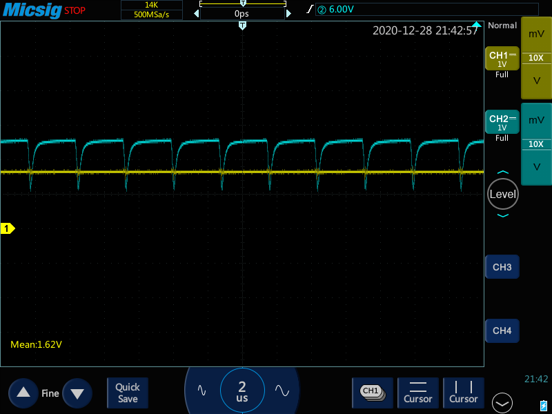
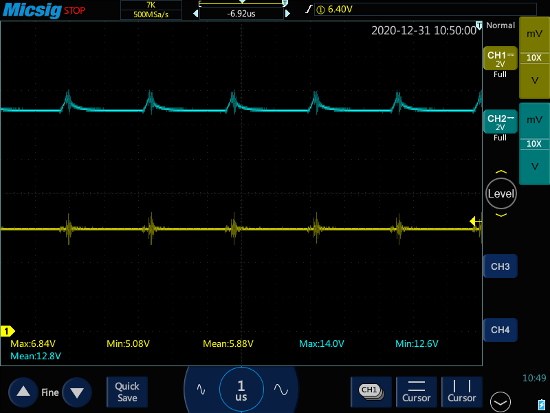
The duty of the pulse at SW node is small. And here is the measured waveform.

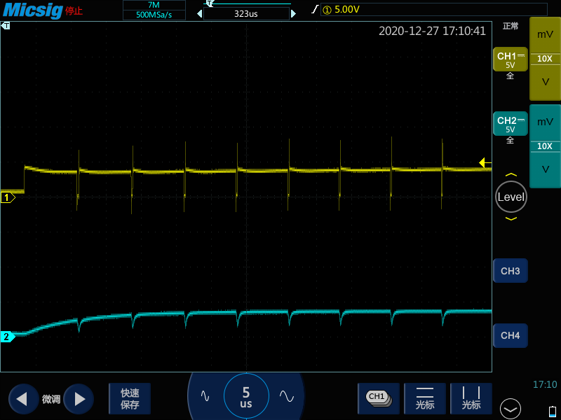
The yellow waveform is V(SW) and the blue waveform is V(OUT1). The duty of V(SW) is quite large, and it seems to keep such a large duty till the output voltage reaches its target value. Please see the figure below.

I have no idea how to explain this phenomenon. Does the circuit operate normally? I don't think so. What's wrong with it?

  • Hello,

    I found that the voltage at pin 6 (ss) is 1.62V, while the datasheet says it should be 2V when the circuit is in steady state.

    What's wrong with the IC?

  • Hi ZD,

    I will need to check with the expert for this device. I'll let you know their response.

    Regards, Jason

  • Hi ZD,

    Can you also share the schematic of the PCB?

    Can you verify that the FB resistors and ripple component connections are made? Do you have a waveform of the FB voltage?

    Thanks, Jason

  • Hello, Jason

    Please see the schematic of the pcb below.

    And the coresponding schematic of the circuit is

    The waveform at SS pin and FB pin is

    The yellow curve is the waveform at SS pin, its mean value is 1.62V. The blue curve is the waveform at FB pin.

  • Hi ZD,

    What is the min and max voltage on the feedback pin? I can't tell from your waveform.

    It looks like the primary voltage goes between 11.3V to 8.8V? What do the two secondary output waveforms look like?

    Please check the feedback connection and the ripple injection values and connections. 

    Is this happening on 1 board or several boards?

    Regards, Jason

  • Hello, Jason

    The yellow curve is V(OUT1), the blue curve is V(FB) and the pink curve is V(SW). Their max and min value is displayed in the figure.

    And here is the figure of V(OUT2), the yellow curve, and V(OUT3), the blue curve.

    I have made only one board.

  • Hi ZD,

    Thanks for sending the waveforms.

    Checking your design on Webench (report attached), it looks like you would need 65uH of primary inductance. From your schematic, it looks like you may be using 17uH? Please check to see if the transformer inductance.

    Also, from your layout, it looks like the injection network capacitor (C3) trace, may be picking up noise from the SW node. 

    You can also try disconnecting the secondary components for VOUT2 & VOUT3 and see if VOUT1 regulates to 8V. Since for flybuck the main regulation comes from the primary side of the circuit. 

    Then if you can get the primary to regulate correctly, add VOUT2 components to see if it regulates, and then VOUT3.

    LM5160_Flybuck_E2E.pdf

    Regards, Jason

  • Hi ZD,

    Any update? I  am hoping that you have resolved your issue.

    I will close this post. If assistance is still needed you can reply and re-open.

    Regards, Jason