This thread has been locked.

If you have a related question, please click the "Ask a related question" button in the top right corner. The newly created question will be automatically linked to this question.

TPS65084: A voltage drop occurred in buck 3 for TPS650842 design

Part Number: TPS65084
Other Parts Discussed in Thread: CSD87381P

Hi All,

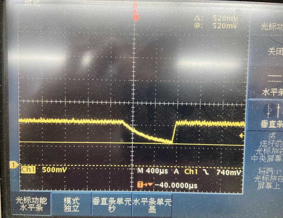
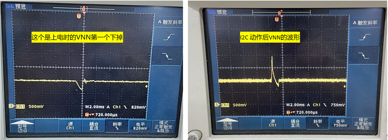
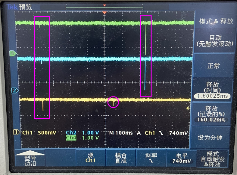
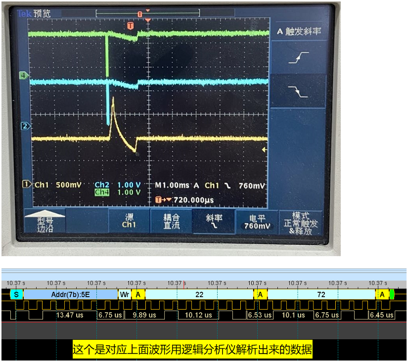
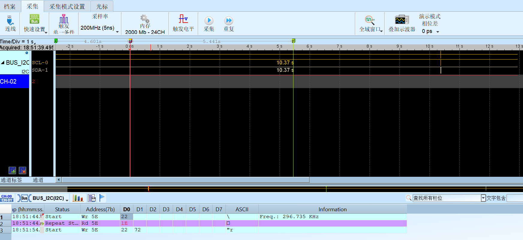
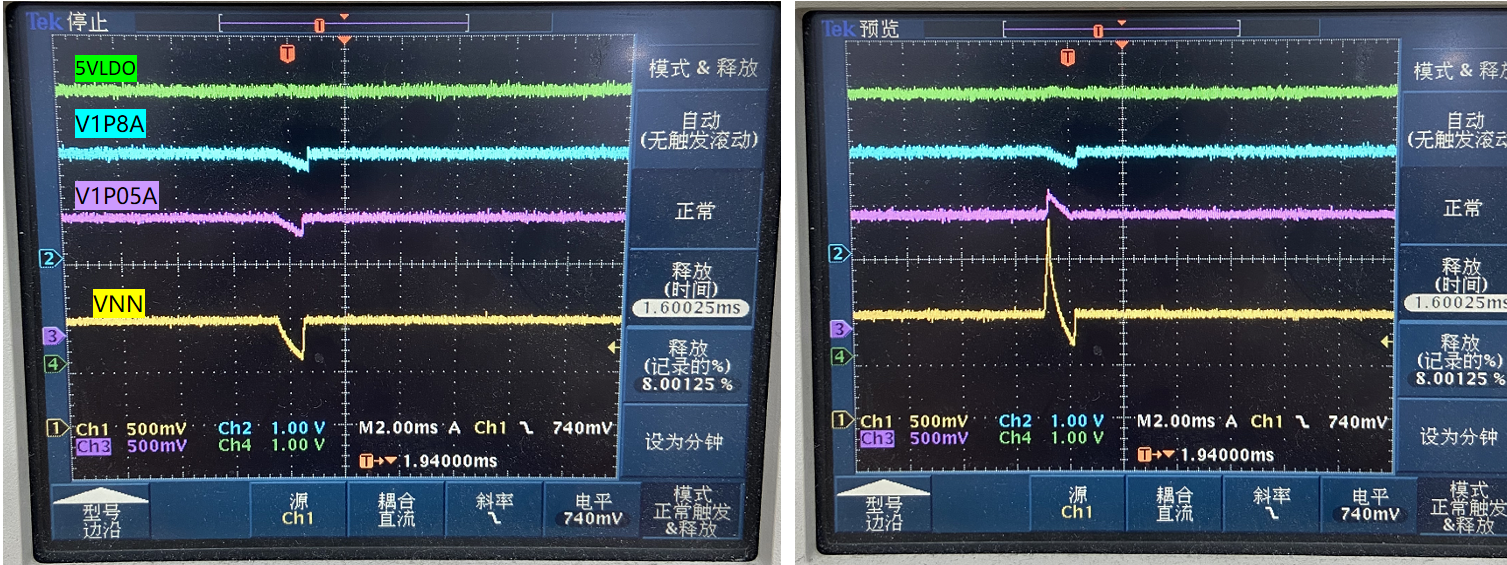
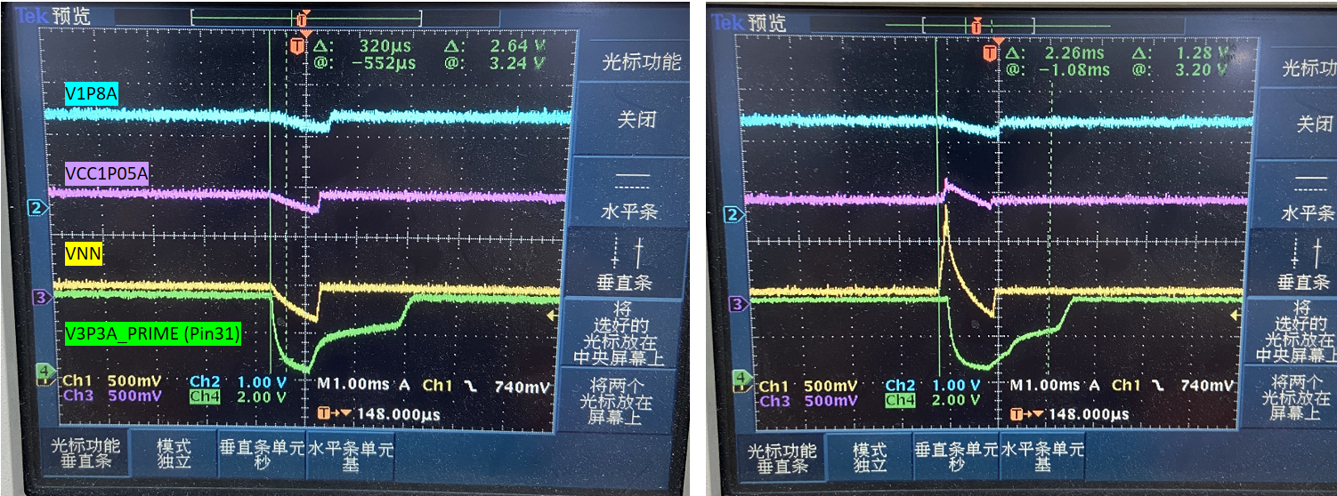
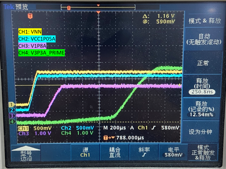
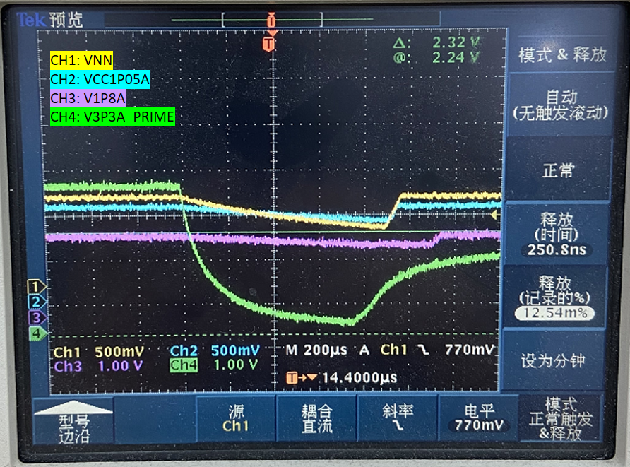
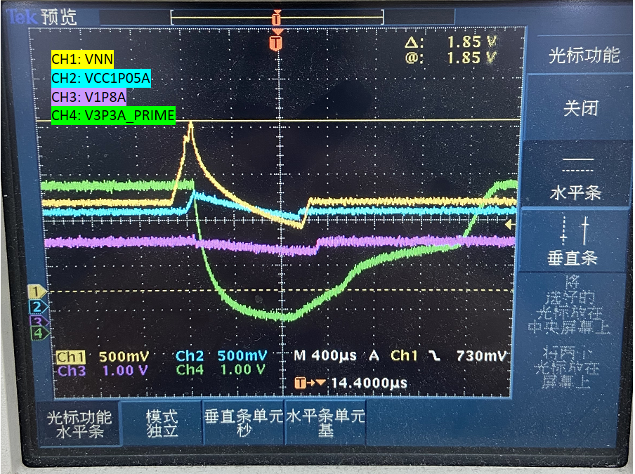
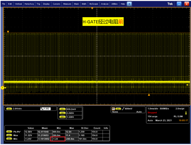
One of our projects uses the TPS650842 PMIC product. When powering on, a voltage drop occurred in VNN (Buck3) , which will cause power down later.

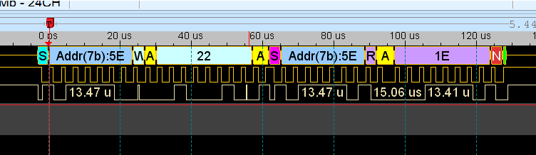
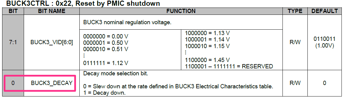
We have read this voltage drop through I2C, and then try to adjust the VNN voltage, but the VNN voltage will eventually reach about 1.8V (the specification shows that VNN voltage is 1.05V@typ. and 1.45V@max.), then the system is powered off.

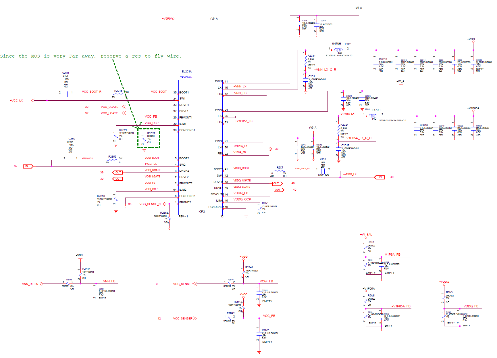
Can u help to analyze the reason for this problem? I added the schematic diagram of my circuit design and the drop waveform to the below.

Thanks,

Best Regards

Schematic diagram:

Drop waveform:

  • Hello,

    In the waveform it does not look like VNN is reaching 1.8V, can you clarify what you are doing to cause VNN to hit 1.8V? How frequently does this rail drop and cause the device to reset? Are the other rails dropping at the same time? If you could provide a scope shot of LDO5V, VNN, V1P05A and V1P8A when the shutdown happens I should be able to provide some more information.

    Best regards,

    Layne J

  • Hi Layne,


    Now I added a picture of an error in adjusting the VNN voltage, as follows:


    After a drop appears in VNN line in the above figure, I got the following data VNN=0.65V from the PMIC I2C. Due to the level limitation of the logic analyzer trigger, VNN cannot be put in. The scope shot is as follows:

    Corresponding to the waveform on the right of the first picture, I got a waveform and the data analyzed by the logic analyzer: VNN should be 1.05V, but now it is up to 1.8V. The waveform is as below:

    The logic analyzer reduces the display ratio, and we can see two pieces of data appear during the entire power-on process. As following picture:

    Q: How frequently does this rail drop and cause the device to reset? 

    A: Now we can see a drop in VNN line when power is on, and then it will cause the system powered off. The probability is 100%.

    Q: Are the other rails dropping at the same time?

    A: VNN, VCC1P05A, V1P8A will also appear a drop. In addition, the waveform of +V3P3A_PRIME (Pin31) captured by the logic analyzer will also shows a drop occured. I guess that the abnormal VNN caused the PMIC to work abnormally.

    Thanks,

    Best Regards

  • Hello,

    Sorry for the delay but I will need a little more time to review the data you provided here. I will provide an update tomorrow.

    Best regards,

    Layne J

  • Hi Layne,

    Thanks a lot.

    If any more detailed information was needed, don't hesitate to tell me.

    Kind Regards

  • Hello,

    Can you zoom in more on the scope shot containing VNN, VCC1P05A, V1P8A, and V3P3A_PRIME? I want to see if the device is following the proper sequencing.

    Is the device under any type of load when the output voltage drops? 

    In the screenshot you provided it looks like you are trying to write 0x72 to register 0x22, is this correct? If that is correct, 0x72 is is a prohibited value for register 0x22. Please reference the TPS650842 datasheet in section 5.10.9. That section will provide the valid register values that you can write to that register.

    Best regards,

    Layne J

  • Hi Layne,

    Sorry to reply u so late, we just had our Traditional Festival for the past few days.

    There were two findings in following tests:

    a. When VNN is fixed at 1.05V, the first drop will not be seen, and the system can be powered on normally.
    b. Disconnect I2C, the first Drop will not be seen, and it can be powered on normally, but the subsequent stability test failed.

    The response to your question is as follows:

    1. Enlarged timing diagram of VNN, VCC1P05A, V1P8A, and V3P3A_PRIME

    Enlarged view of the first drop:

    2. When a drop occurred, the system did not add any additional load, just doing the normal boot runing.

    3. According to the specification, 0x72=01110010, and the last bit is decay mode selection. So the effective bits are 0111001=39, ~1.07V. (But from the waveform point of view, it was finally adjusted to about 1.8V)

    Thanks,

    Best Regards

  • Hello,

    Can you confirm where you got that copy of the datasheet from? I have checked two different downloads of the datasheet that I have on my end and it looks like you have a version that does not match what I am seeing for that register. According to the documentation I have the maximum allowed value for the BUCK3CTRL register is 0x43. 

    Best regards,

    Layne J

  • Hi Layne,

    The screenshot of BUCK3CTRL in my previous reply comes from the datasheet of TPS650840 (Page 49). I added it to the attachment, pls check it.

    I cannot find the detailed information from the datasheet of TPS650842, can u share it to me?

    Thanks,

    Best Regards

  • Hello,

    That datasheet is for TPS650840 which is slightly different than TPS650842. To gain access to the TPS650842 datasheet please go to this page and click the "Request Now" button next to the line that says "Full data sheet and other information are available". Once you complete this request, someone will review your request and grant you access to the TPS650842 datasheet which will show you the difference in this register.

    Best regards,

    Layne J

  • Hi Layne,

    Thanks a lot.

    Can we keep focus on the voltage drop in VNN (Buck3)? All the following work like VNN voltage adjustment and other testing are to solve the problem. 

    Best Regards,

    Lumina

  • Hello,

    I believe you may be seeing the strange behavior due to the incorrect bits you are setting to the BUCK3CTRL register. Please review the valid bits seen in the screenshot from the TPS650842 datasheet below and use this when trying to set the output voltage to see if the behavior changes.

    Best regards,

    Layne J

  • Hello Layne,

    A new problem appeared in this project about TPS650842, the problem is described as follows:

    We replaced a new set of MOS for BUCK6, which is used to power the memory. During our debugging process, we found that there would be a power drop problem of S3, and the signal of LX was as low as -1.8V (input power is 8V).

    Is there any way to reduce the noise of this LX? We tried to added a snub circuit (using 4.7 ohm/4700pF, or 2.2 ohm/4700pF), but get no imporment for this problem.

    Thanks,

    Best Regards

  • Hi Lumina,

    Can you provide a scope shot as well as clarify which of the LX pins you are seeing the negative voltage transient at?

    Best regards,

    Layne J

  • Hi Layne,

    I have added the whole scope shot, pls check it.E117B_V23-T波形.rar

    In our test we found that the TPS650842 power drop will occur about 1 minute after the system waking up (the load test does not done, and the power drop problem occurs when waking up from sleep).

    We connect a 4.7R resistor in series to the H-Gate and L-Gate of Buck1, Buck2, Buck6; add a snub circuit 2.2R+4700pF to SW; it can reduce the probability of power failure, but the problem will be reappeared after about 4 hours later. 

    We measured that the peak value of the SW signal is too large, while we changed the resistance value of the snub circuit and got not improved.

    In the test, it is found that the minimum value of IC end of H-Gate and L-Gate is Buck1 VCC=-2.36V, Buck2 VGG=-1.48V, Buck6 VDDQ= -1.24V. All of them are beyondthe requirement of -0.3V in the specification, and the value of SW is around -1.5V.

    Attached are some measured waveforms, please help us to see how to make the min value in the spec range.

    Thanks,

    Best Regards

  • Hi Layne,

    During the test last night, we found that when a 12V adapter is used for power supply (at this time, the input of PMIC's VSYS and MOS is 12V), the problem will occur as described before. But with two strings of batteries for power supply (up to 8.7V, MOS and VSYS are also 8.7V), the power drop problem will not occur. Any suggestions for this?

    Thanks,

    Best Regards

  • Hi Lumina,

    I am checking with our design team regarding the absolute minimum on the DRVLx and DRVHx pins to ensure this transient will not be an issue.

    To clarify on your last post, which issue are you referring to? Do you mean that you do not see the the negative voltage on the DRVxx pins when using the 8.7V supply?

    Best regards,

    Layne J

  • Hi Layne,

    The problem in my previous reply refers to a power drop problem of S3, and the signal of LX was as low as -1.8V (input power is 8V).

    Thanks,

    Best Regards

  • Hi Layne,

    We are ready for production of this project, can we now ignore whether this value (the signal of LX was as low as -1.8V) is within the range described in the spec? We want to know what can we do to lower this value. Is there any suggestions for it?

    Thanks,

    Best Regards

  • Hi Lumina,

    I am going to reach out to one of the designers for this device to check on this negative value and provide an update tomorrow.

    Best regards,

    Layne J

  • Hi Layne,

    Thanks a lot and looking forward to your reply.

    Best Regards

  • Hi Lumina,

    Can you provide a zoomed in scope shot of the LX pin voltage? I want to see how long the transient for this negative voltage is happening for each switching pulse.

    Best regards,

    Layne J

  • Hi Layne,

    The attachment is the waveform of VCC, VGG, VDDQ, pls check them.

    TPS650842_Transient.rar

    We are now encountering a new problem. When playing through HDMI, after unplugging the HDMI cable, the CPU will get stuck, which can last up to tens of seconds, but it can automatically recover later.

    Today I replaced the MOS CSD87381P on the VCC to another MOS AON6934A, and the system worked normally (two pieces were replaced in total). I tried to adjust the parameters of MOS and PMIC (using CSD87381P), but didn't solve this. So how can I do to adjust the parameters to use CSD87381P normally?

    I added my circuit schematic to the attachment, and hope it will be helpful for u to analyze the problem.

    TPS650842_SCH.pdf

  • Hi Lumina,

    I am currently out of office for a holiday, I will follow up on this thread on Monday.

    Best regards,

    Layne J

  • Hi Lumina,

    Layne is OoO currently, thank you for your patience.

    Did you have any scope shots of the new issue?