Hello,
I am trying to use LM74500-Q1 as ideal diode controller to realize power input reverse protection.
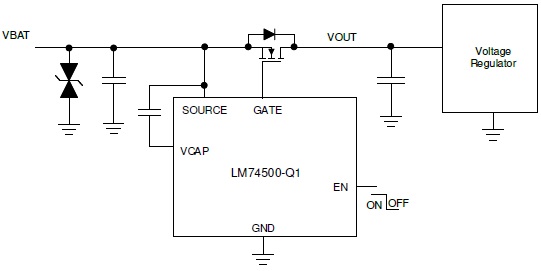
The schematic is basically the same as "typical application schematic" in the datasheet with the following modifications.
1. Pin #1 (EN) and pin #5 (SOURCE) are tired together.
2. The capacitor between pin #5 (SOURCE) and pin #4 (VCAP) is 1uF/50V X7R ceramic capacitor.
3. Voltage of VIN can be any of 5V, 12V and 24V, load current can be up to 7V.
4. MOSFET used with LM74500-Q1 is SiRA80DP.
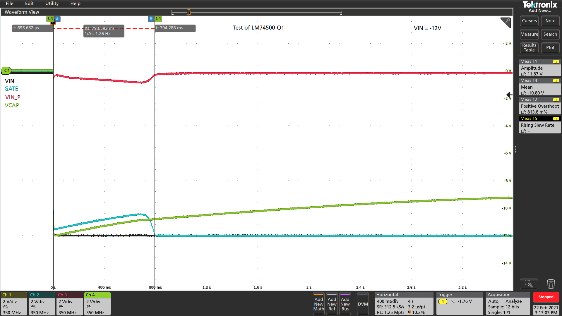
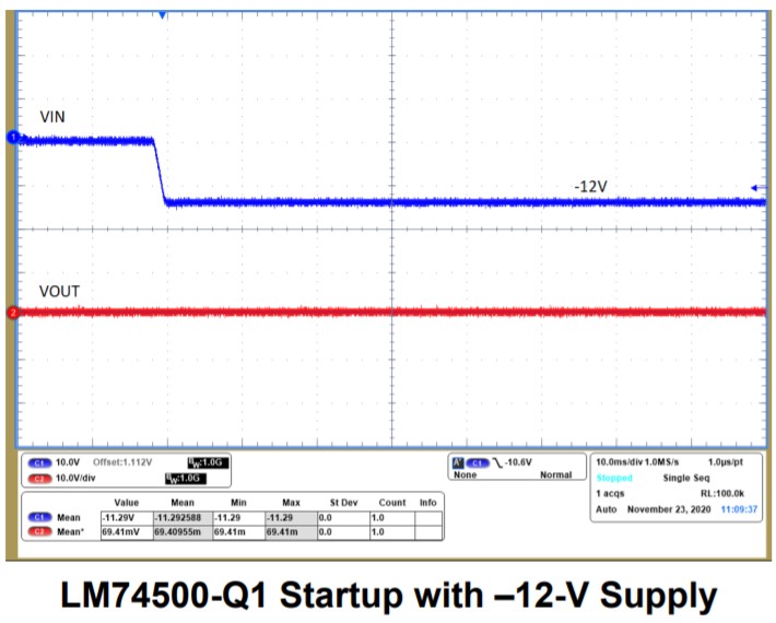
When I tried to connect negative voltage from its input, I found two interesting phenomena.
1. The GATE signal becomes higher than input voltage (SOURCE) for a short period of time (around 1 to 2 seconds), this caused a voltage dip on output. According to the chip's datasheet, the charge pump and gate drive will not work when EN pin voltage is less than the threshold. In our cause, EN is tied with SOURCE, so it always has a negative voltage. I am wondering if there is any reason which can cause the GATE signal become higher than SOURCE momentarily?
2. VCAP finally becomes about 2.5V higher than VIN when VIN is -5V, VCAP becomes about 7V higher than VIN when VIN is -12V. Does that mean the charge pump is still supplying current to the external capacitor even when EN pin voltage is negative (tied with SOURCE), not sure if there is any possible reason for this.
In the waveforms below, black: VIN (-5V and -12V respectively), blue: GATE, red: VOUT, green: VCAP