This thread has been locked.

If you have a related question, please click the "Ask a related question" button in the top right corner. The newly created question will be automatically linked to this question.

UCC27211: High side gate not activating

Part Number: UCC27211
Other Parts Discussed in Thread: SN6501, UCC27282

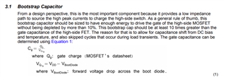
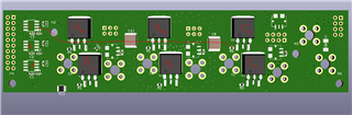
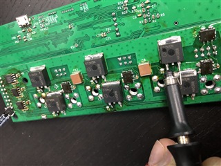
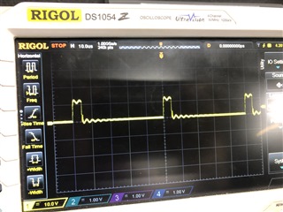
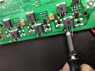
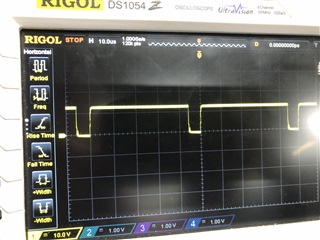
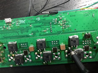
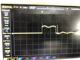
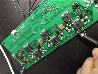
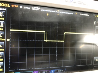
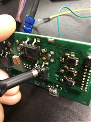
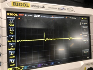
I have designed a power stage 3-phase driver card using the UCC27211 as the gate driver. I have tested the setup in a controlled environment using a function generator at 3.3V levels to drive the gate LI / HI inputs of the UCC27211. From my oscilloscope experiments, I can see that only the low-side gate is being activated by the device. The high side is not driving the high side MOSFET gate. Is there some issue with the bootstrap circuit? I didn't find much recommendation for bootstrap circuitry in the device datasheet, but all I have done is experiment with different values of bootstrap capacitors, with no success. The MOSFETs I am using (IPB072N15N3GATMA1) have a gate charge of approximately 70 nC, for reference. I have posted the schematic here for reference. Any advice on debugging this and figuring out why the high side drive is not working as expected? 

 7411.schematic.pdf

  • Hello Justin,

    Thank you for the interest in the UCC27211. For the high side MOSFET gate drive output to operate, the HB to HS bias needs to be charged to beyond the UVLO start threshold. For the bootstrap capacitor to charge, the power train switch node and driver HS pin needs to switch to close to ground for the boot cap to charge from VDD through the boot diode.

    Confirm that the HS pin or switch node is close to ground potential which should happen when the LO output is driving the low side MOSFET. Also confirm if there is at least 8V on the driver HB to HS pin for the high side bias and VDD for low side bias.

    The only other concern would be to make sure the driver LI and HI signals are switching from ground to beyond the turn on thresholds which is ~2.8V. A 3.3V logic drive will be adequate.

    Confirm these basic operations and provide an update if you have any additional concerns.

  • Thanks for your reply. 

    Please help me to clarify some things

    Confirm that the HS pin or switch node is close to ground potential which should happen when the LO output is driving the low side MOSFET

    Does this mean that I have to toggle the LI pin at least once before the HI pin will trigger an appropriate output on HO? 

    Also, do I have to do this every time I am switching? i.e., do I always need to be doing the PWM/PWMN strategy where either the high or low side are always on? For example, can I just leave the LI pin low, while continuously PWM-ing the HI pin? Or is this not physically possible with this device? 

    Also confirm if there is at least 8V on the driver HB to HS pin for the high side bias and VDD for low side bias.

    Do I check this with a voltmeter, and only after toggling the LI input at least once? 

  • Hello Justin,

    For the 1st question. The HB-HS capacitor is charged from VDD when the HS pin switches to ground, of is at ground potential (or very close). Tis normally happens when the low side FET turns on from the LO output being turned on with the LI signal.

    For the HB-HS capacitor to stay charged it has to be refreshed by the switch node switching to ground, normally from switching the low side FET. The high side drive, HO will not operate if the HB-HS capacitor is not charged above the HB UVLO threshold. It is not possible to only switch the high side output, and not the low side with a typical bootstrap circuit for the high side bias.

    There is a way to operate the high side only, but it required a dedicated floating high side bias circuit which can be implemented using a small simple solution with the SN6501 transformer driver from TI.

    Confirm if this addresses your questions, or you can post additional question on this thread.

    Regards,

  • Richard,

    Thanks for your reply here. I understand now. I am going to modify my switching strategy and see if I can switch the high side in this way then. Do you know how long after switching the switch node to ground that the bootstrap capacitor will hold the charge and be able to switch the high side? 

    Additionally, can you help me to confirm the size of my bootstrap capacitor, given the previously stated 70 nC gate charge, and given that I am running at 12V for VDD? 

    I saw an app note (SLUA887) that said this:

    In my case, this would be roughly 60 nF I think. Would 0.1uF be a good place to start? 

  • Hello Justin,

    Since you are looking at an application that may have long HO on times or low frequency, I would refer you to the UCC28272 datasheet which is a similar 100V half bridge driver but has more detail guidance on sizing the bootstrap capacitor. The driver IC HB quiescent current will discharge the bootstrap capacitor over time which you should account for that. Look at the application example section which includes guidance for the bootstrap capacitor based on frequency and duty cycle. Use the IC parameters from the UCC27211, and the design steps in the UCC27282 datasheet.

    The 100nF cap you mention is adequate for supplying the MOSFET Qg but may need to be increased to hold up from the quiescent current over time. Also if you have a gate to source resistor that will discharge the bootstrap capacitor as well. Add the current thru the gate to source resistance to the IHB in the equation.

    Confirm if this addresses your question, or you can post additional questions on this thread.

    Regards,

  • Hi, I managed to get things working a little better and now I'm doing a complementary PWM strategy that seems to be running the motor ok at low speeds. Now I keep burning up my phase C UCC27211 driver. I have probably burned up 3 drivers already and pretty much all at high speeds. Phase C is the farthest half bridge away from the UCC27211 also. 

    Do you think it could be a layout problem? Perhaps it's pushing the gate signal distance a bit too much. 

    This is a 2-layer board and all the signals from the 'mother' board come in on the header on the left side. I can also share layout files here if useful. What is the most common cause of a UCC27211 heating up and failing to work under operating conditions? 

  • Hello Justin,

    Layout can definitely be a concern regarding stress to the driver. I do have one question. When you mention complimentary PWM strategy, is there a single PWM control signal and operating the driver with a complimentary high side and low side output? I ask this question only because it is important to have some dead time in the driver outputs between the high side and low side on times.

    With a long gate driver to MOSFET trace loop, there is a good chance that there may be voltage overshoot and undershoot on the gate driver outputs relative to VDD and ground, or relative to HB and HS.

    Confirm with scope probes that the LO, HO and HS pins are within the datasheet recommended operating range. There may be excessive voltage on the gate driver outputs or possibly the HS pin.

    If there is voltage overshoot on the driver outputs, this can be improved by increasing the resistance from the driver to the MOSFET. This will slow the switching dV/dt and help dampen the voltage ringing caused by the layout trace inductance.

    Confirm if this addresses your questions, or you can post additional questions on this thread.

    Regards,

  • Hi Richard,

    Thanks for the reply. Yes, I am using a microcontroller that has built in dead-time settings for the pwm. Currently I am using about 500ns of dead time between switching transitions of high side and low side, so I'm not worried about shoot-through in this case. 

    I will try and get some more scope results on these pins in the following days to see if I can find abnormal conditions. 

    Is there any suggestions to debug a failed chip and see which part of the circuit is failing? (e.g. measure resistance or something across certain pins?). 

  • Hello Justin,

    To confirm which pins might be failing, which will be useful information I suggest comparing the resistances of the pins most likely to fail in a converter with a fresh unused driver sample.

    Measure resistance of LO pin to ground (VSS), HO pin to HS pin, HB pin to HS pin, and HS pin to ground (VSS). Measure with a DVM with the ground lead of the meter referenced to either VSS or HS. Also measure VDD to HB in the diode test mode to see if the boot diode is failed. VDD is the anode of the boot diode.

    Regards,

  • Hi Richard,

    I have 3 failed chips in total, and I did some comparisons of them with a new chip. 

    Unfortunately there was not a lot of consistency between the failed chips, but here are some notable differences when compared to the new chip: 

    1 failed chip had infinite resistance from HB,HO,HS to VSS(GND), and this is the same as the new chip. However, the other failed chip had 1.16M, 8M, and 2M, respectively for those pins. 

    Also, the measurement of HO to HS was around 7.5M on the new chip, and one of the failed chips measured about 22M here. 

    HB to HS was 0.98M on a new chip, and open-circuit on one of the failed chips

    HS to GND was 27M on a new chip and open-circuit on one of the failed chips, and 2.1M on another failed chip

    At least one of the failed chips had a short-circuit on the diode between VDD and HB. The new chip measured 0.65V, whereas the other two failed chips measured 0.65V and 0.58V. 

    With my knowledge, I'm not sure this info gives me conclusive evidence about potential failure modes, but perhaps you can provide some advice. 

    Here are some more details. I was doing some oscilloscope experiments with a new chip and got these results on phase C, where the gate driver is always failing:

    Probing high side MOSFET gate to source, during switching, with no load:

    high side gate source - no load switching

    Low side:

    low side gate to source - switching with no load

    I also probed before the gate resistors on each, with a noisier result:

    Do the spikes on the high side drive seem to be the culprit? They are upwards of 20V, at least from the scope. 

    Can I protect from failures using some zener or TVS diodes across gate and source? 

    Finally, here is an example of the low side switching that happens during loading (with a motor attached, but at low power):

    Finally, I wanted to mention that if I run the motor at low speeds, everything seems fine and the chips are all cool to the touch. When I increase the duty cycle, the chips seem to start heating up and eventually phase C gate driver seems to be the first one to fail. 

    What could be the reason for heating up substantially during operation at higher loads and failing? I'm assuming it is transients that are starting to damage the chip internally. 

    Any advice is appreciated on trying to resolve the issue. 

    Thanks. 

  • Hello Justin,

    Thank you for the update. With the pin comparison measurements, to me it is a bit inconclusive since many of the measurements are either very high impedance or showing out of range. The one you mention with the boot diode difference, VDD to HB, on the device that has the short you mention I assume the VF is very low, not 0.6 to 0.7V. Please confirm.

    The plots you show with the voltage spikes on the drive are a concern. There may be Vgs perturbations from the MOSFET switching which may false trigger the MOSFETs.

    With the long distance from the driver to at least 2 of the MOSFETs this is not unusual.

    One thing that helps with this is to have some capacitance right on the MOSFETs gate and source pins. This helps stabilize the Vgs from the miller charge that is transferred to the gate during switching. With long traces from the driver to MOSFET, the driver has limited ability (due to the trace inductance) to clamp the Vgs.

    Also, can you confirm that the driver LI and HI pins do not have voltage spikes that may false trigger the driver? If there is noise on LI and HI try adding a small R/C filter, start with 50 Ohms and 100pF.

    Regards,

  • Richard,

    In regards to your first question, yes the device that has the boot diode difference has a VF of essentially 0V. The other devices have 0.58V and 0.65V, and the new part has a 0.65V boot diode measurement. 

    I understand about the Vgs perturbations and the MOSFET false trigger potential. I could probably patch in some capacitance in my current setup, but it would be hard to add R/C filters to the HI/LI pins in my current setup. 

    The main question I have now is what could be causing the chips to heat up during operation at higher loads? Do you know of what can cause them to get hotter when at higher loads? Is the fact that they are getting hot indicative of damage or out of range voltage spikes on certain pins? 

  • Justin,

    There are a couple of possibilities. At higher loads the power MOSFETs will have higher temperature rise, the close location of the driver to the MOSFETs could be thermal conduction back to the driver.

    If there is false triggering of the driver this will increase the frequency of the driver which will increase which will increase the driver power dissipation.

    Regards,

  • Hi Richard, 

    I don't think that the MOSFETs are rising in temperature at all, or at least not significantly. Whereas the driver chips seem to be rising pretty quickly up to > 70 deg C. The false triggering could be a possibility too, as you mentioned. 

    Do you know if heat would be produced if the maximum voltage specifications were repeatedly being violated on the bootstrap or HO/LO pins? Or would heat in this case be indicative of irreparable damage? 

  • Hello Justin,

    It is possible if the voltages on the IC pins are beyond the datasheet recommended ranges that there could be additional current into the IC. I would confirm the HO, HS including negative voltage, LO & HO including overshoot/undershoot.

    Also confirm my previous suggestion that the gate driver is not false triggering and generating additional pulses that are not intended. Even narrow output spikes from the driver will add to the gate drive loss.

    Regards,