This thread has been locked.

If you have a related question, please click the "Ask a related question" button in the top right corner. The newly created question will be automatically linked to this question.

BQ78350-R1: NACK after the slave address

Part Number: BQ78350-R1
Other Parts Discussed in Thread: BQ78350, BQSTUDIO

Hi,

I am trying to communicate with BQ78350-R1 using STM32F091,via SM BUS protocol.

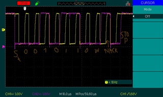
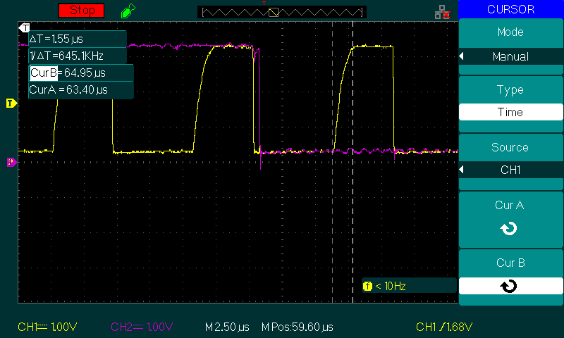
I am getting a NACK after the slave address(0x16), What can be the reason for the NACK?

I am running the clock at 60khz,and clock stretching is enabled. The Cumulative clock low extended time is 4ms. How to know that BQ78530 is ready for communication? The data line and clock line are pulled up to 3.3V using external pull up resistor. The VEN pin is generating pulses of(1.5V) does this indicate that the device is still booting or does it do it even after boot-up? Currently I have powered up BQ78350 using external power source (2.5V).

  • Hi Vinay,

    The VEN pin pulses are normal - this is used to control an external FET to sample the battery stack voltage so that the resistor divider is not always drawing current. I recommend using a logic analyzer with the EVM to capture the SMBus waveforms using BQStudio, then compare these to the SMBus for your MCU to see what might be different. You should not be getting a NACK after the slave address.

    Best regards,

    Matt

  • Hi,

    I don't have access to EVM. So can you share a link to those waveforms if you have it. But I would like to share the waveform which I am getting on the board.

    the address is 0x16 right shifted by 1 and write mode. I am trying to read the serial number of the device ie by default=1, So I am sending 1 byte of data 0x1C(smbus command specified in reference manual).

    Also, I wanted to know if do we require level shifter? Since the MCU's VCC is 3.3V and BQ78350's VCC is 2.5.

    2nd observation- The trise time on data line is 1.55us but the max allowed as per smbus specification it is 1000ns can this be the reason? So i reduced the pullup from 2.2k to 1K and there was no communication.

  • Hi Vinay,

    Your address 0x16 should not be shifted. See this thread for an example logic analyzer capture: https://e2e.ti.com/support/power-management/f/power-management-forum/977536/bq78350-r1-nack-problems-after-the-repeated-start

    Best regards,

    Matt

  • Hi,

    Thank you.

    Yeah I realized that it was a mistake and I corrected it now I was able to communicate. I was successful in reading device name and toggle leds. But that is the method followed right? In I2C communication ie the slave address should be left shifted ? So the slave address should be 0x16》1=0x0B and then when left shifted we get 0x16 as final address.