This thread has been locked.

If you have a related question, please click the "Ask a related question" button in the top right corner. The newly created question will be automatically linked to this question.

UCC28740: The major difference between UCC28740 and UCC28742?

Part Number: UCC28740
Other Parts Discussed in Thread: UCC28742

Hi Teams

I am seeking a 85~230AC to 24V/75W solution for customer. And both UCC28740 and UCC28742 is my candidate.

  • My first questions is which part more sutiable for highe power level flyback and why?

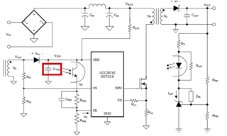
I noticed the major difference between these two device is pacakge and HV startup pin.

  • Could you explain more about the advantage of HV startup pin compara to tradistional start-up resistor type like UCC28740?
  • UCC28740 have lower no load power consumption. I want to know what lead to such difference?

Thanks in advance.

  • Hello Gabriel,

    Thank you for your interest in the UCC28740 and UCC28742 flyback controllers.

    Both devices are equally suited for the 24-V, 75-W application. One does not have a performance advantage over the other in this regard.

    As you noted, the UCC28740 has a larger package and a high-voltage start-up pin (HV), whereas the UCC28742 is in a smaller package without HV start-up. The UCC28740 incorporates a high-voltage JFET to provide about 250 uA to charge up the VDD capacitance relatively quickly, and is switched off after start-up to save no-load standby power .  This additional JFET increases the size of the controller and so the larger SOIC-8 package is required.

    On the other hand, the UCC28742 has no start-up FET and so relies on an external resistor string from the bulk voltage to charge the VDD capacitance.  This reduces cost and the allows a smaller SOT-23 package, however it requires a trade-off of start-up speed vs. additional stand-by power dissipation in the start-up resistors.  Their values are determined by the longest tolerable start-up time with a given VDD capacitance at the lowest input voltage.  Once this value is fixed, the power dissipation at high line is always present, even at no-load, hence the higher stand-by power with UCC28742. 

    Regards,
    Ulrich

  • Hi Ulrich

    Thanks for your comments.

    As customer only need no load power consumption less than 0.1W, it seems UCC28742 could also meet their requirement.

    I suppose UCC28742 will be more cost effective choice? 

    Few further questions for UCC28742:

    • In fault condition that MOSFET can't turn-on. Will CVDD keep being charged and exceed the voltage tolenrence of VDD Pin? Will this pin be damaged in this condition?
    • In application note " Minimize Standby Consumption for UCC287xx Family" it indicated that X-cap have impact to standby power consumption and could calculated by below formulate. I want to know what Rx mean and how to obtain this value?

  • Hello Gabriel,

    Yes, the UCC28742 should be able to meet the 0.1W no-load stand-by limit and will be more cost effective.

    In the case of a MOSFET fault where it cannot switch, there is no danger to the VDD or to CVDD. At start-up, IC bias current is about 1.5uA whereas the start-up resistor will provide maybe 15uA or more to charge CVDD.  When the VDD voltage reaches ~21V, the IC will turn on and try to drive the MOSFET into switching.  The IC bias current go up to about 2mA and this level is much higher than the few uA available through the VDD charging resistance.  If there is no switching, VDD will sink to the ~8V UVLO threshold and bias current will drop to 1.5uA again. Then the start-up resistor will charge VDD back up to ~21V, and the cycle will repeat indefinitely as long as the MOSFET is unable to switch.  There will be no overvoltage stress on the VDD net.

    In the "Pdis" formula above, Rx is the "bleeder" resistance across the X-cap, which is needed to discharge any voltage across the cap within 1 or 2 seconds (depending on which safety standard is being used).  The value of the X-cap is chosen based on how much capacitance is needed to help reduce differential mode conducted EMI noise.  Once this value is known, the Rx value is chosen to meet the X-cap discharge time based on the RC time constant required.  Therefore, Rx = tau/Cx, where tau = discharge time constant and Cx = total value of all X-caps.

    Note: the higher the X-cap value, the better the EMI performance, BUT the lower the Rx value that will be needed to discharge it within the time limit allowed.  Lower values of Rx result in higher stand-by dissipation at high line (230Vac), so Cx should be as low as possible to do the job.

    Total stand-by power = ( no-load input power of UCC28742 converter + dissipation of Rx ), must be < 0.1W.

    Regards,
    Ulrich

  • Hi Ulrich

    Thanks for your comments.

    Are this "bleeder" resistor place in series with X-cap? 

    General speaking which part of power consumption will be dominated factor to total standby power? Dissipation in "bleeder" resistor or start-up resistor or IC bias current?

  • Hello Gabriel,

    The bleeder resistance is placed in parallel with the X-cap.  It's purpose is to "bleed" the charge from the X-cap after the AC line voltage is removed, such as by unplugging the line cord, so that high voltage does not stay present across prongs of the line cord plug to avoid shocking people who may touch them. Usually, this "bleeder" resistance is not a single resistor (although it can be), but typically consists of 2,3,4, or more smaller resistors in series in order to spread out the highest voltage stress across each of them. Surface-mount components have a "limiting element voltage" rating that must be observed.  A single resistor rated for 400Vdc across it would be very large, so usually, it is broken up into several smaller components in series.  This series string of resistors is placed across the X-cap and always dissipates power.  Highest power is at high line, and forms part of the stand-by power consumption.

    Stand-by power consumption is not dominated by any one factor.  The X-cap bleeder forms a significant portion, the VDD charge-up resistance (sometimes referred to as trickle-charge) forms a significant portion (similar to the bleeder), primary IC bias power is a significant portion, and the secondary-side shunt-regulator contributes a significant portion. These portions are not necessarily equal in power, but all are significant contributors.  These are easily quantifiable since they are mostly the summation of V^2/R and VxI calculations.

    Lesser contributors include bulk-cap leakage current, primary MOSFET leakage, output cap leakage, any minimum output pre-load necessary for no-load stability, and the stand-by switching losses incurred by switching the power conversion (at low frequency) simply to keep the regulator alive and regulating even at no-load. These are not so easy to determine, since leakage currents and no-load frequency cannot be predetermined, but must be measured or estimated after a prototype is constructed and tested.  

    Regards,
    ulrich