Other Parts Discussed in Thread: LM3409
Sorry for my delayed response of the related question attached to this one.
I have been going back and forth with the circuit (trying to fix the problem of the related question) and seems I have some different output and signals, without any noticiable change at least as far as I can remember. Anyway the output signal is far from being right.
As I stated in my other question,
- Led Load in each channel is: 4 leds in 2parallel string (2 led in series+ 2 leds in series). It is designed for 2.5 A por string (5 A per channel), Vin 12 V Vout 7. 8 volts
- EN1 and EN2 strobes channel 1&2 and channel 3&4, respectively. This signal is 100 Hz, 500us-2 ms width, depending on the application
The circuit is the same than the related question
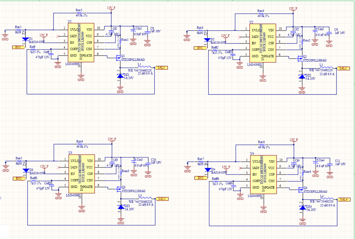
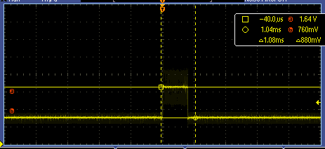
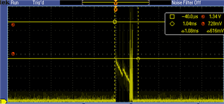
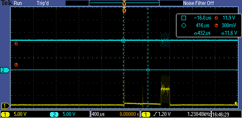
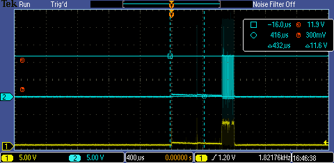
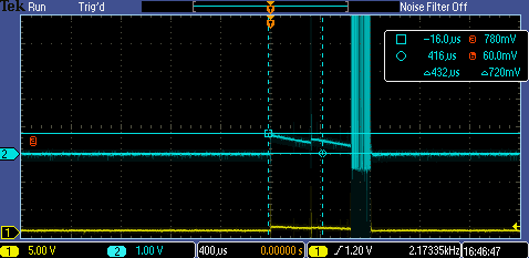
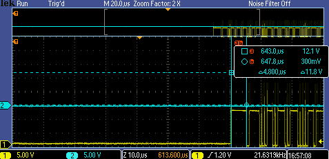
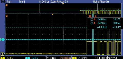
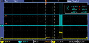
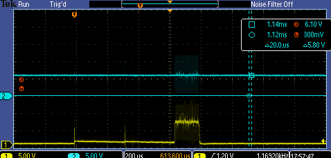
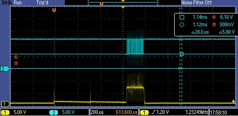
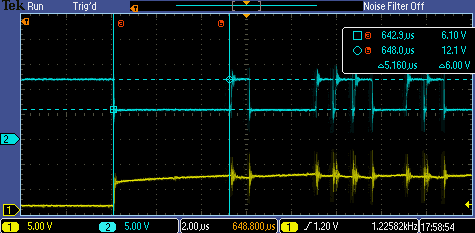
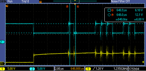
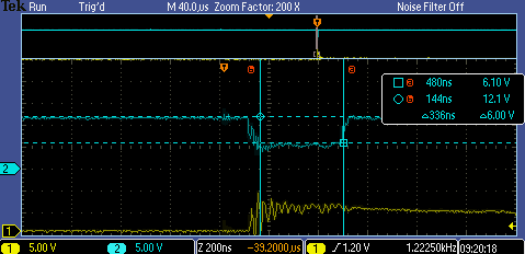
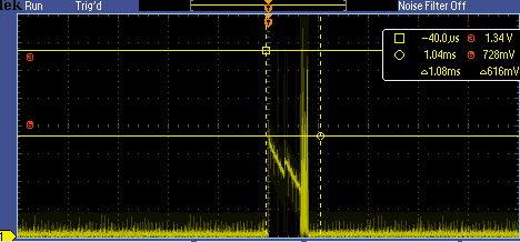
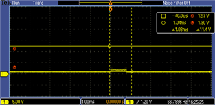
The output and the different voltages in the diferent nodes of the channel 1 are as follows
Output voltage:
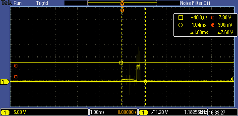
Coff node:
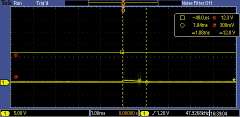
UVLO node (see that V_uvlo=1.3v when En1=0V and V_uvlo=2.1v when EN1=12V:
Dont really know what is happening. Anyone can guide, please?
Regards